

Assembling structure of camera module and assembling method for reducing dimension of camera module
A technology of camera module and assembly method, which is applied in the direction of image communication, color TV parts, TV system parts, etc., can solve the problem that the assembly process cannot meet the market requirements, achieve size reduction, increase support strength, The effect of improving optical performance
- Summary
- Abstract
- Description
- Claims
- Application Information
AI Technical Summary
Problems solved by technology
Method used
Image

Examples
Embodiment Construction
[0019] In the following description, numerous specific details are set forth in order to provide a thorough understanding of the present invention. However, the present invention can be implemented in many other ways different from those described here, and those skilled in the art can make similar extensions without violating the connotation of the present invention, so the present invention is not limited by the specific implementations disclosed below.
[0020] Secondly, the present invention is described in detail by means of schematic diagrams. When describing the embodiments of the present invention in detail, for convenience of explanation, the schematic diagrams are only examples, which should not limit the protection scope of the present invention.
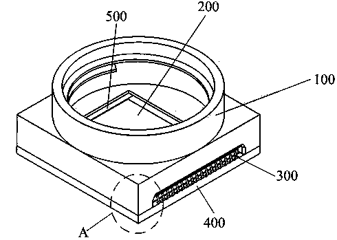
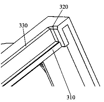
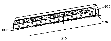
[0021] In order to make the above-mentioned purposes, features and advantages of the present invention more obvious and understandable, the following in conjunction with the attached Figure 1~Figure 4 The assembly struct...
PUM
 Abstract
Description
Claims
Application Information