
AC-DC chip and high-voltage free-wheel diode integrated chip structure and power module group
A technology of freewheeling diodes and integrated chips, which is applied in circuits, electrical components, and electric solid-state devices, can solve the problems of power drive module volume, unfavorable use, etc., reduce volume costs, improve production efficiency, and overcome technical barriers Effect
- Summary
- Abstract
- Description
- Claims
- Application Information
AI Technical Summary
Problems solved by technology
Method used
Image

Examples
Embodiment 1
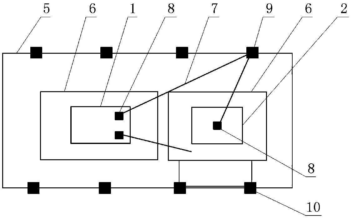
[0024] Such as figure 1 As shown, in this embodiment, the first chip 1 is provided with an integrated structure, that is, the first chip 1 adopts an AC-DC chip including a control logic circuit and a power MOS device, wherein the first chip 1 and the second chip 2 They are respectively arranged on two independent lead frames. The first chip 1 is arranged on the lead frame where it is located through insulating glue, and the anode of the second chip 2 is connected to the lead frame where it is located through conductive glue or solder paste. On the first chip 1 The other pad 8 leads out the drain of the power MOS device in the first chip 1 through the metal lead 7, and is connected to the lead frame where the second chip 2 is located to form a connection with the anode of the second chip 2.
Embodiment 2
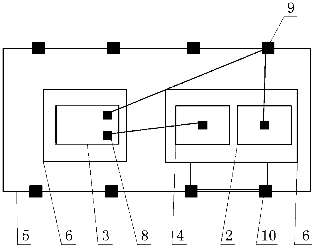
[0026] Such as figure 2As shown, in this embodiment, the first chip 1 is set as a split structure, that is, the first chip 1 includes a third chip 3 including a control logic circuit in AC-DC and a fourth chip 3 including a separate power MOS device. Chip 4. Wherein, the third chip 3 and the fourth chip 4 are respectively arranged on two independent lead frames, the third chip 3 is provided with at least two bonding pads 8, and one bonding pad 8 on the third chip 3 passes through the metal The lead 7 is connected to the high-voltage power supply pin 9 of the plastic package 5, another pad 8 on the third chip 3 is connected to the gate of the fourth chip 4 through the metal lead 7, and the drain of the fourth chip 4 is connected to the gate of the second chip 2. anode. In this embodiment, the fourth chip 4 and the second chip 2 are jointly arranged on the same lead frame, and the drain of the fourth chip 4 and the anode of the second chip 2 are connected to the lead frame th...
Embodiment 3
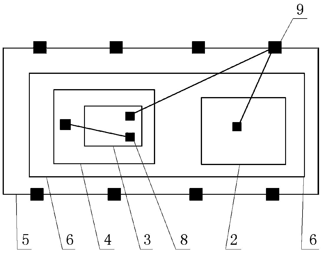
[0029] Such as image 3 As shown, in this embodiment, the first chip 1 is set as a split structure, that is, the first chip 1 includes a third chip 3 including a control logic circuit in AC-DC and a fourth chip 3 including a separate power MOS device. Chip 4. Wherein, the fourth chip 4 and the second chip 2 are jointly arranged on the same lead frame through conductive glue or solder paste, and the drain electrode of the fourth chip 4 and the anode of the second chip 2 are connected to the lead wire through conductive glue or solder paste. frame, the third chip 3 is arranged on the gate surface of the fourth chip 4 through insulating glue, at least two pads 8 are arranged on the third chip 3, and one pad 8 on the third chip 3 passes through a metal lead 7 Connect the high-voltage power supply pin 9 of the plastic package 5, another pad 8 of the third chip 3 is connected to the gate of the fourth chip 4 through the metal lead 7, and the lead frame protrudes from the plastic pa...
PUM
 Abstract
Description
Claims
Application Information