Supercharge Your Innovation With Domain-Expert AI Agents!

Method for defect-free copper filling of hole in part carrying member and plating device

A component-carrying, unfilled technology, applied in the processing of printed circuit components, electrical components, insulating substrates/layers, etc., can solve problems such as ineffective operation, poor performance, and irregular growth process of copper material 310, To achieve the effect of saving material costs

Inactive Publication Date: 2019-02-12
AT & S AUSTRIA TECH & SYSTTECHN AG
View PDF13 Cites 0 Cited by
  • Summary
  • Abstract
  • Description
  • Claims
  • Application Information

AI Technical Summary

Problems solved by technology

These defects 350 directly lead to an irregular growth process of the copper material 310 as gaps 345 remain during the growth process, and eventually lead to irreparable cracks and / or voids
However, the flow of chemical additives cannot effectively reach the gap 345 between the plurality of copper material portions 310
Therefore, as in Figure 4b As seen in , in the final component carrier 400 there are still defects such as cracks and / or voids in the filled copper material 310
As a result, filling hole 520 with conductive material is hampered and cannot be done in an efficient manner.
[0011] Because processes using chemical additives often do not work efficiently, performance is often poor and defects remain
Furthermore, chemical additives lead to additional costs and are generally harmful to the environment, and so far no effective process for defect-free filling of holes in component carriers has been provided

Method used


Image

  • Method for defect-free copper filling of hole in part carrying member and plating device
  • Method for defect-free copper filling of hole in part carrying member and plating device
  • Method for defect-free copper filling of hole in part carrying member and plating device

Examples


Embodiment Construction

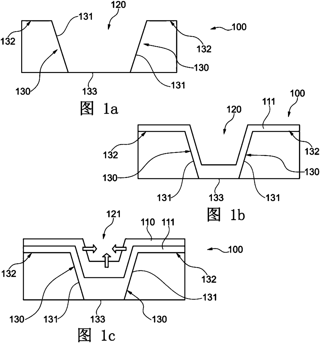
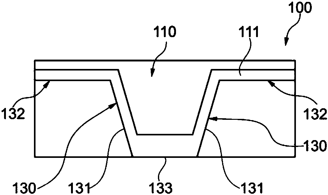
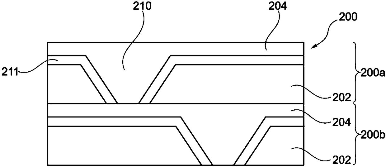
[0075] Before describing the exemplary embodiments in more detail with reference to the drawings, some basic considerations on the basis of which the exemplary embodiments of the present invention have been arrived at will be summarized.

[0076] According to an exemplary embodiment of the invention, the filling capacity of the holes in the component carrier is increased and a better reliability of the component carrier, in particular of the PCB, is achieved with regard to function. Usually, the concentration of copper ions in the plating environment is around 35g / L. On the one hand, when the concentration is lower, the formation of defects such as cracks increases. On the other hand, when the copper concentration is too high, not all of the copper is soluble anymore, and crystallization of copper occurs. Copper concentrations in the high range of 50 g / L to 80 g / L, especially about 65 g / L would not be considered appropriate in a plating environment due to the increased likeli...


PUM

PropertyMeasurementUnit
Thicknessaaaaaaaaaa

Abstract

The invention discloses a method of using copper (110) to fill a hole (120) formed in a part carrying member (100). The method includes: i), forming a conductive material layer (111) covering at leasta part of a surface (131) of a wall (130) which defines the hole (120); ii), using the cooper (110) for a plating process including bath to partly cover the layer (111) at least and to partly fill unfilled volume (121) of the hole (120) at least, wherein the bath includes copper ions, especially Cu2+, with concentration within a range of 50-75g / L, especially 60-70g / L.

Description

technical field [0001] The invention generally relates to the filling of holes in component carriers. In particular, the invention relates to filling holes in component carriers with copper by plating, while avoiding defects in the copper-filled holes. Furthermore, the invention relates to a device for carrying out the method. Furthermore, the invention relates to a component carrier produced by this method. Background technique [0002] Electronic assemblies and circuits including electronic components are typically built on a component carrier such as a printed circuit board (PCB). The manufacturing process of so-called multilayer component carriers usually involves filling the holes in the component carrier with an electrically conductive material, such as copper. [0003] The density and complexity of electronic components continues to increase, while the holes in the component carriers (such as laser drilled holes) are getting smaller and the aspect ratios (aspect ra...

Claims


Application Information

Patent Timeline
IPC IPC(8): H05K3/42
CPCH05K3/422H05K2203/072H05K3/423H05K2201/0344H05K2201/09563H05K2203/1476Y10T29/49165H05K3/0094H05K3/0026H05K3/0055H05K1/0298H05K3/241H05K3/244H05K3/4644
Inventor 王大学淩绮冰安妮·泰
Owner AT & S AUSTRIA TECH & SYSTTECHN AG
Features
  • R&D
  • Intellectual Property
  • Life Sciences
  • Materials
  • Tech Scout
  • Unparalleled Data Quality
  • Higher Quality Content
  • 60% Fewer Hallucinations
Learn More