Thyristor packaging method

A technology of silicon encapsulation and encapsulation, which is applied in the field of thyristor encapsulation, can solve the problems that the chip, the lead frame and the upper and lower encapsulation casings cannot be guaranteed tightly, and the encapsulation casing is warped, so as to improve the anti-collision performance and stability. The effect of enhancing unity

Inactive Publication Date: 2019-02-26
浩明科技(中山)有限公司
View PDF2 Cites 1 Cited by
  • Summary
  • Abstract
  • Description
  • Claims
  • Application Information

AI Technical Summary

Problems solved by technology

However, during the packaging process, due to the gap between the upper and lower package shells at the lead frame, the force on the outer edge of the package may cause the package to warp, which cannot ensure that the chip, lead frame and the upper and lower package shells are tightly combined, leaving gap

Method used


Image

  • Thyristor packaging method
  • Thyristor packaging method
  • Thyristor packaging method

Examples


Embodiment Construction

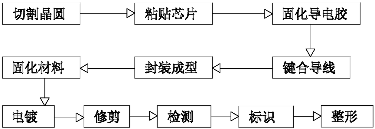
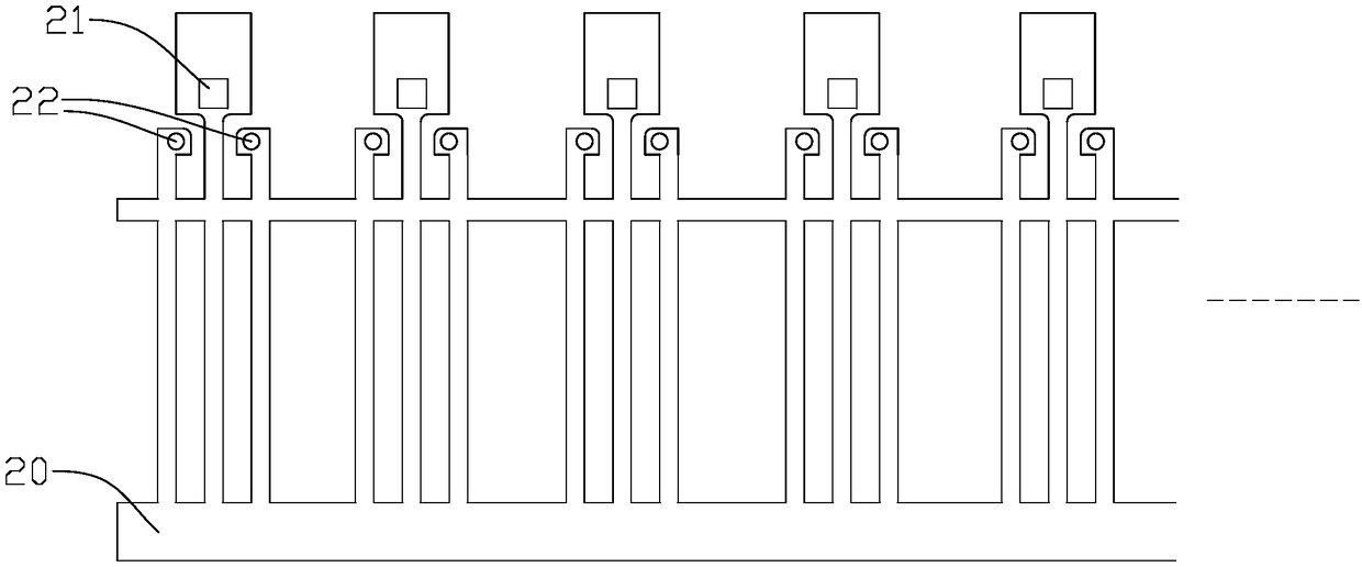
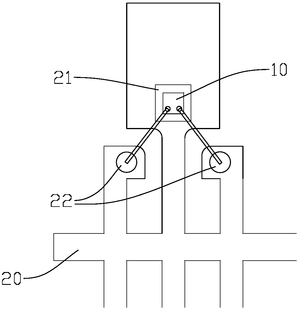
[0025] refer to Figure 1 to Figure 4 , a thyristor packaging method, including a wafer, a plurality of chips 10 on the wafer and an external metal plate is arranged on the chip 10, a lead frame 20, the lead frame 20 is provided with several chips 10 for fixing The fixing point 21 and the welding point 22 corresponding to the outer metal disc include the steps of:

[0026] Cutting the wafer: cutting the wafer so that the wafer is divided into several independent chips 10;

[0027] Sticking the chips 10: fixing several chips 10 on different fixing points 21 of the lead frame 20 through conductive glue;

[0028] Curing conductive adhesive: heating to cure the conductive adhesive;

[0029] Bonding wires: connect the external metal plate on the chip 10 to the corresponding soldering point 22 on the lead frame 20 through wires;

[0030] Encapsulation molding: the encapsulation material is injected to surround the chip 10 and part of the lead frame 20 to form an encapsulation cas...


PUM


Abstract

The invention discloses a thyristor packaging method. A thyristor comprises a wafer. A number of chips are arranged on the wafer, and external metal disks and lead frames are arranged on the chips. Anumber of fixing points used for fixing the chips and soldering points corresponding to the external metal disks are arranged on the lead frames. The method comprises the steps that the wafer is cut,and the wafer is divided into a number of independent chips; when the chips are pasted, a number of chips are fixed on different fixing points of the lead frames through conductive glue respectively;the conductive glue is heated and cured; at the step of wire bonding, the external metal disks on the chips are connected with the corresponding soldering points on the lead frames through wires; andat the step of packaging molding, the chips and a part of the lead frames are surrounded by a packaging material through injection molding to form a package casing. According to the method, gaps caused by loose combination of the chips, the lead frames and the package casing can be avoided at the step of packaging molding.

Description

technical field [0001] The invention relates to the field of semiconductors, in particular to a silicon controlled silicon packaging method. Background technique [0002] In the prior art, the thyristor includes a chip and a lead frame, and the packaging is generally completed by machine crimping, argon arc welding, cold sealing and the like. The cold seal is widely used because it requires simple equipment, easy operation, easy maintenance of parts and components, and lower production costs. Cold sealing is to apply sufficient mechanical pressure on the die at room temperature, so that the outer edges of the upper and lower packaging shells can be tightly laminated, thereby achieving the purpose of packaging. However, during the packaging process, due to the gap between the upper and lower package shells at the lead frame, the force on the outer edge of the package may cause the package to warp, which cannot ensure that the chip, lead frame and the upper and lower package ...

Claims


Application Information

Patent Timeline
IPC IPC(8): H01L21/56
CPCH01L21/56H01L2224/48247H01L2224/49171H01L2224/97H01L2924/181H01L2924/00012
Inventor 李长征
Owner 浩明科技(中山)有限公司
Why Eureka
Try Eureka