
Microphone and manufacturing method thereof

A manufacturing method and microphone technology, applied in the field of semiconductors, can solve problems such as affecting the performance of the microphone, and achieve the effects of improving the filling effect, reducing or eliminating weaknesses, and eliminating holes

Active Publication Date: 2019-03-05
SEMICON MFG INT (SHANGHAI) CORP +1
View PDF5 Cites 0 Cited by
  • Summary
  • Abstract
  • Description
  • Claims
  • Application Information

AI Technical Summary

Problems solved by technology

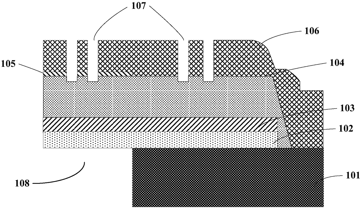
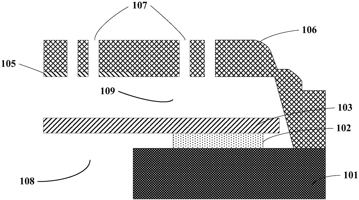
[0006] However, the inventors of the present application have found that after the wet etching process, the first insulating layer 102 and the second insulating layer 104 that need to remain under the support layer 106 will also be removed or partially removed, so that under the support layer 106 Forms unwanted holes that affect microphone performance

Method used


Image

  • Microphone and manufacturing method thereof
  • Microphone and manufacturing method thereof
  • Microphone and manufacturing method thereof

Examples


Embodiment Construction

[0029] Various exemplary embodiments of the present application will now be described in detail with reference to the accompanying drawings. It should be understood that the relative arrangements of components and steps, numerical expressions and values ​​set forth in these embodiments should not be construed as limiting the scope of the present application unless specifically stated otherwise.

[0030] In addition, it should be understood that, for the convenience of description, the dimensions of the various components shown in the drawings are not necessarily drawn according to the actual scale relationship, for example, the thickness or width of some layers may be exaggerated relative to other layers.

[0031] The following description of the exemplary embodiments is illustrative only and is not intended to limit the application, its application or uses in any way.

[0032] Techniques, methods and devices known to those of ordinary skill in the relevant art may not be disc...


PUM


Abstract

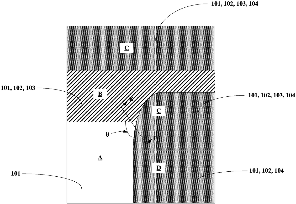
The invention discloses a microphone and a manufacturing method thereof, and relates to the technical field of semiconductors. The method comprises the following steps: providing a substrate structure, wherein the substrate structure comprises a substrate and a first insulating layer covering a part of the substrate; forming a first electrode plate layer, wherein the first electrode plate layer covers a part of the first insulating layer; and forming a second insulating layer, wherein the second insulating layer covers a part of an area of the first insulating layer that is not covered by thefirst electrode plate layer and a part of the first electrode plate layer; wherein, during overlooking, the first electrode plate layer and the second electrode plate layer form an angle, the angle exposes a part of the substrate, and the angle theta of the angle satisfies that theta is greater than or equal to 90 degrees and is less than or equal to 180 degrees. By adoption of the manufacturing method disclosed by the invention, the problem of forming undesirable holes in the microphone can be improved.

Description

technical field [0001] The present application relates to the technical field of semiconductors, in particular to a microphone and a manufacturing method thereof, and more particularly to a micro-electromechanical system (MEMS) microphone and a manufacturing method thereof. Background technique [0002] Figure 1A and Figure 1B A cross-sectional schematic view showing different stages of a conventional manufacturing method of a microphone. [0003] First, if Figure 1A As shown, a substrate structure is provided. The substrate structure includes: a substrate 101, a first insulating layer 102 on the substrate 101, a first electrode plate layer 103 on the first insulating layer 102, and a second insulating layer on the first electrode plate layer 103 104 , the second electrode plate layer 105 on the second insulating layer 104 , and the supporting layer 106 on the second electrode plate layer 105 . The second electrode plate layer 105 and the support layer 106 have through...

Claims


Application Information

Patent Timeline
IPC IPC(8): H04R19/04H04R31/00
CPCH04R19/04H04R31/00H04R2201/003H04R2231/003H04R19/005B81B2201/0257B81B2203/0315B81B2203/0353B81B2203/04B81C1/00166
Inventor 张健闾新明
Owner SEMICON MFG INT (SHANGHAI) CORP
Learn More