PCB production mold
A mold and mold group technology, applied in the electronic field, can solve problems such as low substrate yield, high temperature resistance, and thermal insulation design that do not meet the requirements, and achieve the effect of temperature stability
- Summary
- Abstract
- Description
- Claims
- Application Information
AI Technical Summary
Problems solved by technology
Method used
Image

Examples
Embodiment Construction
[0016] In order to make the above objects, features and advantages of the present invention more comprehensible, the present invention will be further described in detail below in conjunction with the accompanying drawings and specific embodiments.
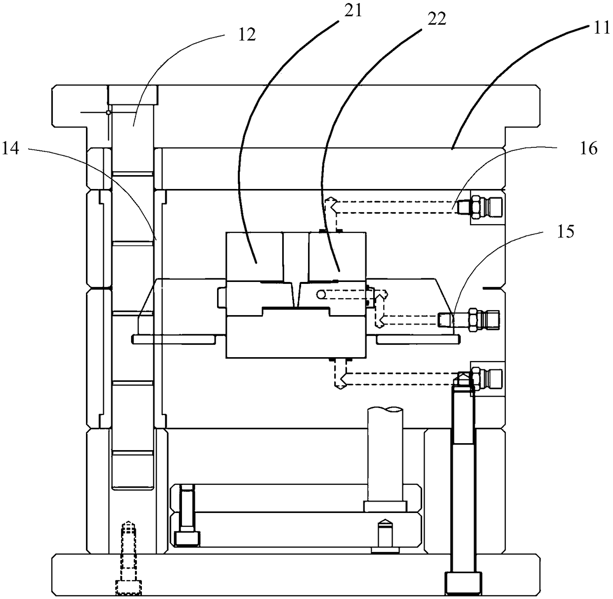
[0017] refer to figure 1 , is a schematic structural diagram of a PCB production mold according to an embodiment of the present invention;
[0018] In the embodiment of the present invention, the targeted circuit board substrate is a substrate material containing PPS material, specifically, a circuit board substrate containing a certain proportion of PPS and GF may be used.
[0019] In the embodiment of the present invention, the circuit board substrate containing PPS and GF materials is subjected to injection molding processing, and the injection molding processing is performed according to design requirements.
[0020] The PCB production mold provided by the embodiment of the present invention includes a first mold set 11 and a...
PUM
 Abstract
Description
Claims
Application Information
 - Generate Ideas
- Intellectual Property
- Life Sciences
- Materials
- Tech Scout
- Unparalleled Data Quality
- Higher Quality Content
- 60% Fewer Hallucinations
Browse by: Latest US Patents, China's latest patents, Technical Efficacy Thesaurus, Application Domain, Technology Topic, Popular Technical Reports.
© 2025 PatSnap. All rights reserved.Legal|Privacy policy|Modern Slavery Act Transparency Statement|Sitemap|About US| Contact US: help@patsnap.com