Semiconductor device
一种半导体、壳体的技术,应用在半导体器件、半导体/固态器件零部件、电固体器件等方向,能够解决安装性存在问题、未考虑散热板翘曲等问题
- Summary
- Abstract
- Description
- Claims
- Application Information
AI Technical Summary
Problems solved by technology
Method used
Image

Examples
Embodiment approach 1
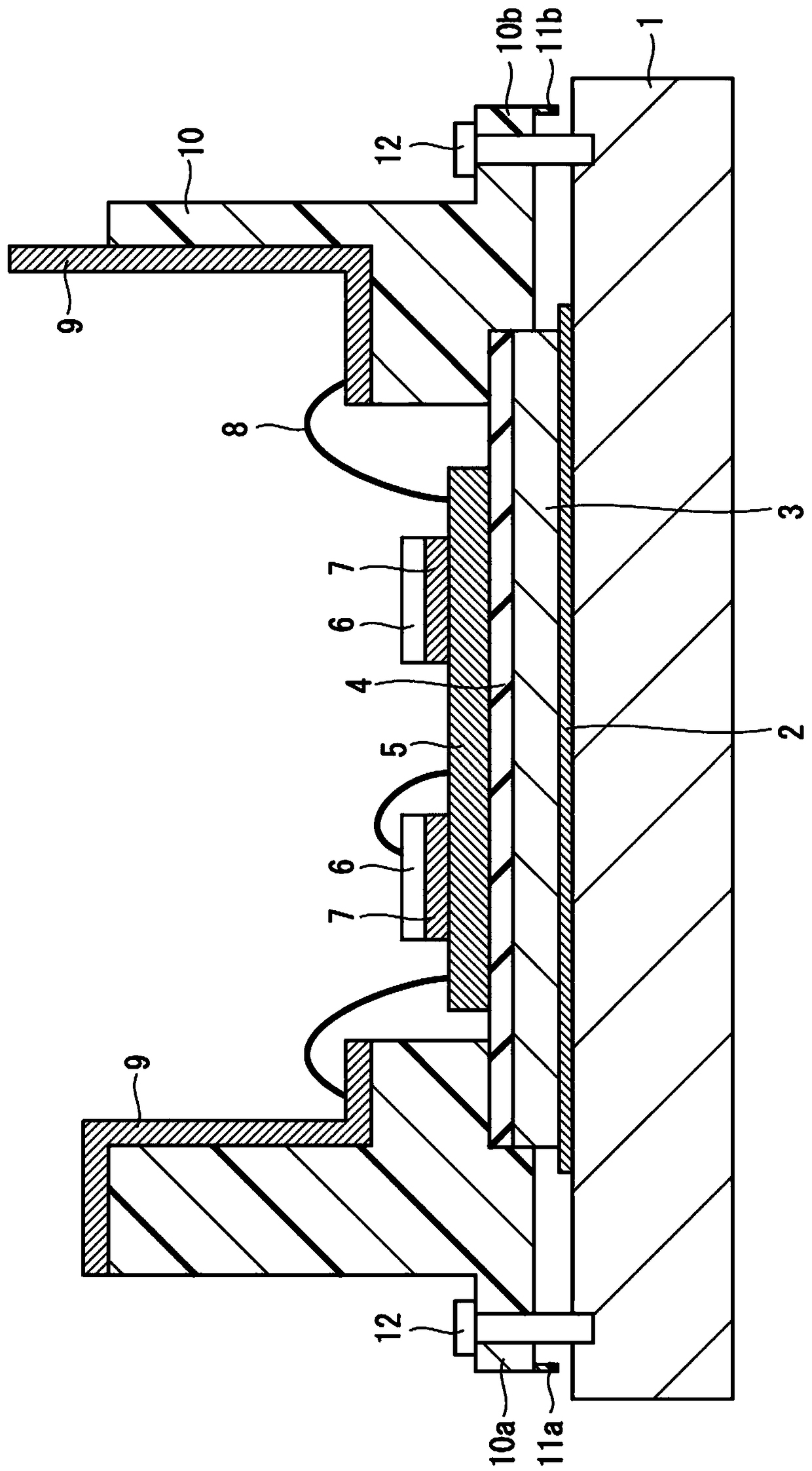
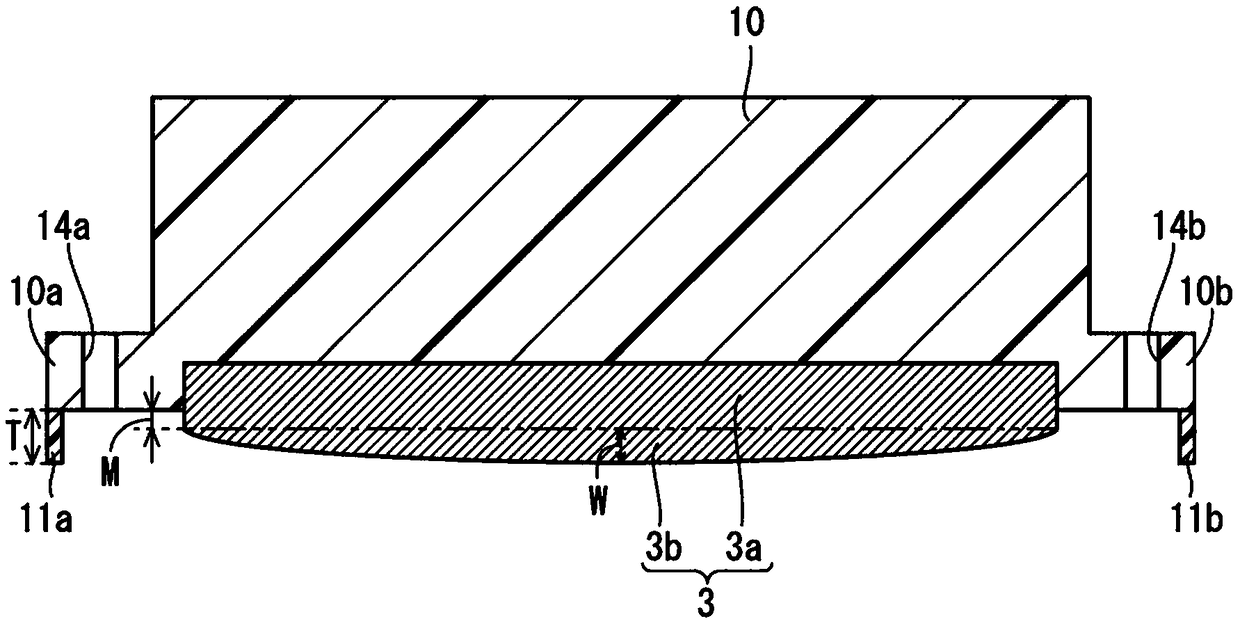
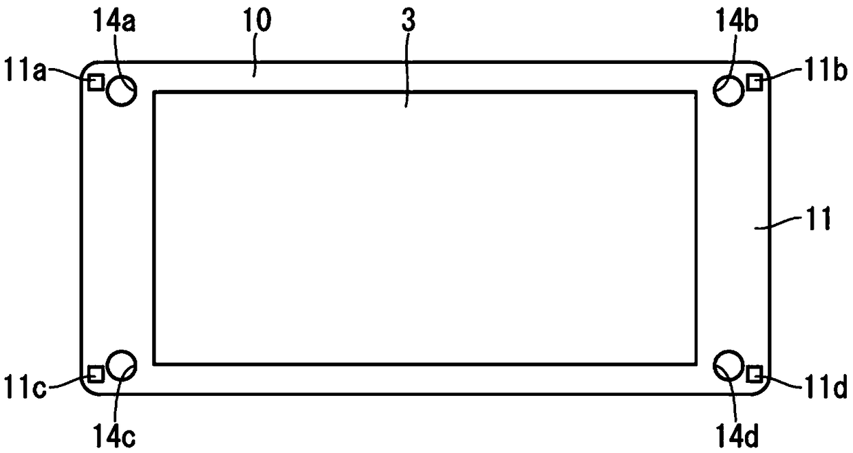
[0035] Hereinafter, the first embodiment of the present invention will be described with reference to the drawings. figure 1 It is a cross-sectional view of the semiconductor device according to the first embodiment. figure 2 It is a cross-sectional view of the semiconductor device in a state where the heat sink 1 is removed. image 3 It is a bottom view of the semiconductor device with the heat sink 1 removed. Figure 4 It is a bottom perspective view of the raised portion 11b and its peripheral portion.
[0036] Such as figure 1 As shown, the semiconductor device is a power semiconductor device, and the semiconductor device has a heat sink 1, a heat sink 3, a housing 10, screws 12, a plurality of semiconductor elements 6, and a plurality of metal terminals 9.
[0037] A heat dissipation plate 3 is arranged on the upper side of the heat sink 1. More specifically, the heat-conducting material 2 is provided on the lower surface of the heat sink 3, and the heat-dissipating plate 3 is...
Embodiment approach 2
[0061] Next, the semiconductor device according to Embodiment 2 will be described. Picture 9 It is a simplified cross-sectional view of the semiconductor device according to the second embodiment in a screw-fastened state. Picture 10 It is a bottom perspective view of the boss 31 and its periphery. In addition, in the second embodiment, the same components as those described in the first embodiment are assigned the same reference numerals, and the description is omitted.
[0062] In Embodiment 2, such as Picture 9 and Picture 10 As shown, the four bosses 31 have a structure that is bent outward due to the stress when the screw 12 is tightened.
[0063] The protrusion 31 is made of, for example, resin such as PPS. The protrusion 31 is provided with a notch 31a extending in the horizontal direction on the side of the mounting hole 14b located at the peripheral portion thereof, and the notch 31a facilitates the bending of the protrusion 31. The notch 31a facilitates the bending o...
Embodiment approach 3
[0068] Next, a semiconductor device according to Embodiment 3 will be described. Picture 11 This is a bottom perspective view of the bump 41 and its peripheral portion of the semiconductor device according to the third embodiment. Picture 12 It is a cross-sectional view of the boss 41 and its peripheral part. In addition, in Embodiment 3, the same components as those described in Embodiments 1 and 2 are assigned the same reference numerals, and descriptions thereof will be omitted.
[0069] In Embodiment 3, such as Picture 11 and Picture 12 As shown, the four bosses 41 have a structure that bends outward due to the stress when the screw 12 is tightened.
[0070] The protrusion 41 is made of resin such as PPS. The convex portion 41 is provided with an inclined portion 41a that is inclined to the mounting hole 14b side with respect to the lower surface of the mounting portion 10b so that the width of the tip portion becomes smaller than the root end portion. The inclined portion ...
PUM
 Abstract
Description
Claims
Application Information
 - R&D
- Intellectual Property
- Life Sciences
- Materials
- Tech Scout
- Unparalleled Data Quality
- Higher Quality Content
- 60% Fewer Hallucinations
Browse by: Latest US Patents, China's latest patents, Technical Efficacy Thesaurus, Application Domain, Technology Topic, Popular Technical Reports.
© 2025 PatSnap. All rights reserved.Legal|Privacy policy|Modern Slavery Act Transparency Statement|Sitemap|About US| Contact US: help@patsnap.com