Measurement method for back-illuminated wafer crystal edge scribing depth

A back-illuminated, crystal-edge technology, applied in semiconductor/solid-state device testing/measurement, electrical components, circuits, etc., can solve problems such as low measurement efficiency, improve product yield, speed up research and development progress, and support reliable data Effect

Active Publication Date: 2019-03-15
SHANGHAI HUALI INTEGRATED CIRCUTE MFG CO LTD
View PDF4 Cites 3 Cited by
  • Summary
  • Abstract
  • Description
  • Claims
  • Application Information

AI Technical Summary

Problems solved by technology

If more crystal edge positions need to be measur

Method used


Image

  • Measurement method for back-illuminated wafer crystal edge scribing depth
  • Measurement method for back-illuminated wafer crystal edge scribing depth
  • Measurement method for back-illuminated wafer crystal edge scribing depth

Examples


Embodiment Construction

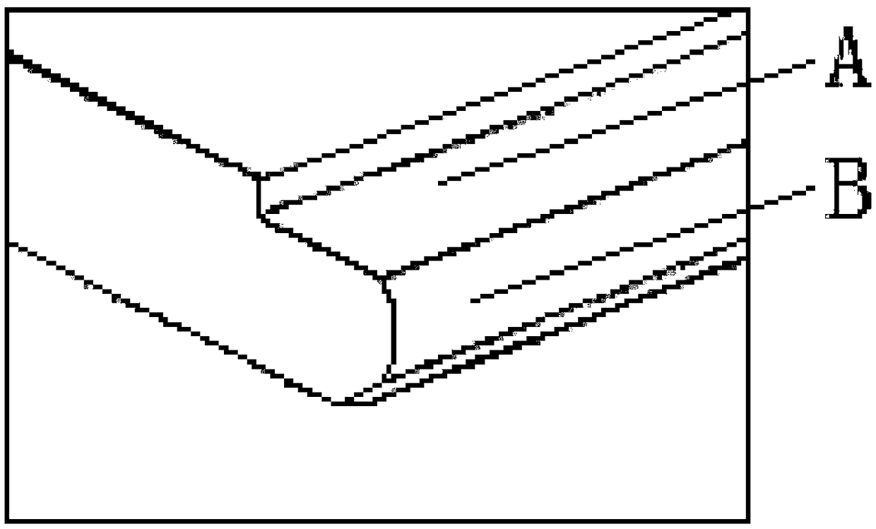
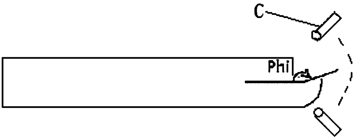
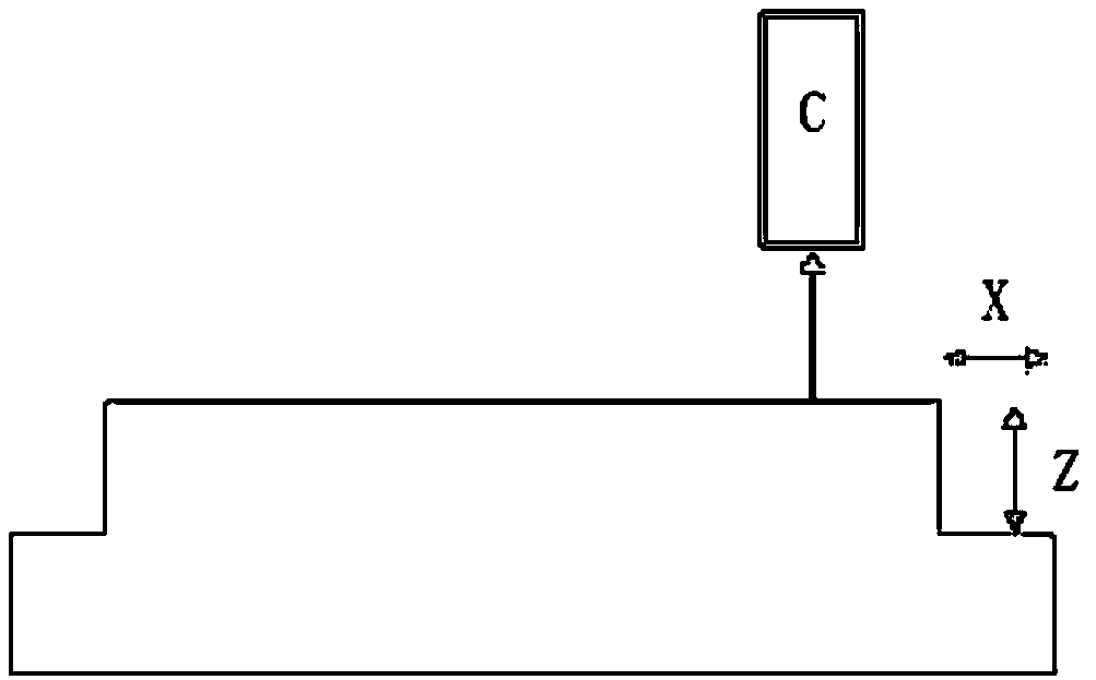
[0037] In the development stage of the back-illuminated wafer back-end process, a sample is selected, and a measurement program is established by using a wafer edge defect detector to scan the edge of the diced wafer to obtain the measurement data of the angular position of the dicing boundary line. Slice the sample and measure the actual scribing depth. The correction coefficient β in the elliptical crystal edge profile model is obtained by substituting the angular position data of the scribing boundary line measured by the crystal edge defect detector and the scribing depth obtained by slice analysis into the relationship function between the scribing depth and the angular position of the boundary line. And according to the correction coefficient β, and the wafer thickness T and other data, a complete elliptical crystal edge contour model corresponding relationship between the scribing depth and the angular position of the boundary line is established.

[0038] In the follow...


PUM


Abstract

The invention provides a measurement method for back-illuminated wafer crystal edge scribing depth. The measurement method comprises the following steps that: adopting a preset way to scan a scribed wafer crystal edge, and obtaining the optical image of the scribed wafer crystal edge; obtaining a scattered signal channel boundary caused by the step structure right-angle side of the scribed wafer crystal edge; measuring an angle position where the boundary of each wafer crystal edge position is positioned; establishing the contour model of the scribed wafer crystal edge; through the establishedcontour model, obtaining a relationship function of scribing depth and the angle position of the boundary; and substituting the measured angle position into the relationship function to calculate thescribing depth of each crystal edge position. Under a situation that the wafer is not damaged, the wafer scribing depth of the back-illuminated wafer on the whole circumference can be effectively measured, reliable data support is provided for the regulation of the scribing technology during a research and development initial stage, a research and development progress is quickened, and product yield is improved.

Description

technical field [0001] The invention relates to the field of integrated circuits, in particular to a back-illuminated wafer edge scribing depth measurement method for inspecting and analyzing defects on a complete wafer during the development of an integrated circuit manufacturing process. Background technique [0002] The back-end process of back-illuminated CMOS image sensor (referred to as BSI CIS) is mainly to bond the CIS wafer carrying the image sensor circuit with the carrier wafer and complete the external interconnection layer process. Before the CIS wafer is bonded to the carrier wafer, the edge of the CIS wafer needs to be diced to prevent peeling caused by incomplete bonding of the wafer due to wafer warpage. Crystal edge scribing is to thin and trim the fixed radius range of the wafer boundary, so that the crystal plane at the scribing position and trimming direction has a step-shaped outline. [0003] In the research and development stage, the slicing method i...

Claims


Application Information

Patent Timeline
IPC IPC(8): H01L21/66
CPCH01L22/12
Inventor 陈超许向辉郭贤权姬峰
Owner SHANGHAI HUALI INTEGRATED CIRCUTE MFG CO LTD
Why Eureka
Try Eureka