
Pixel circuit, pixel driving method and display device

A pixel circuit and circuit technology, applied in static indicators, instruments, etc., can solve problems such as short-term residual image threshold voltage compensation, and achieve the effect of improving hysteresis effect and ensuring consistency

Active Publication Date: 2019-03-19
ORDOS YUANSHENG OPTOELECTRONICS +1
View PDF7 Cites 10 Cited by
  • Summary
  • Abstract
  • Description
  • Claims
  • Application Information

AI Technical Summary

Problems solved by technology

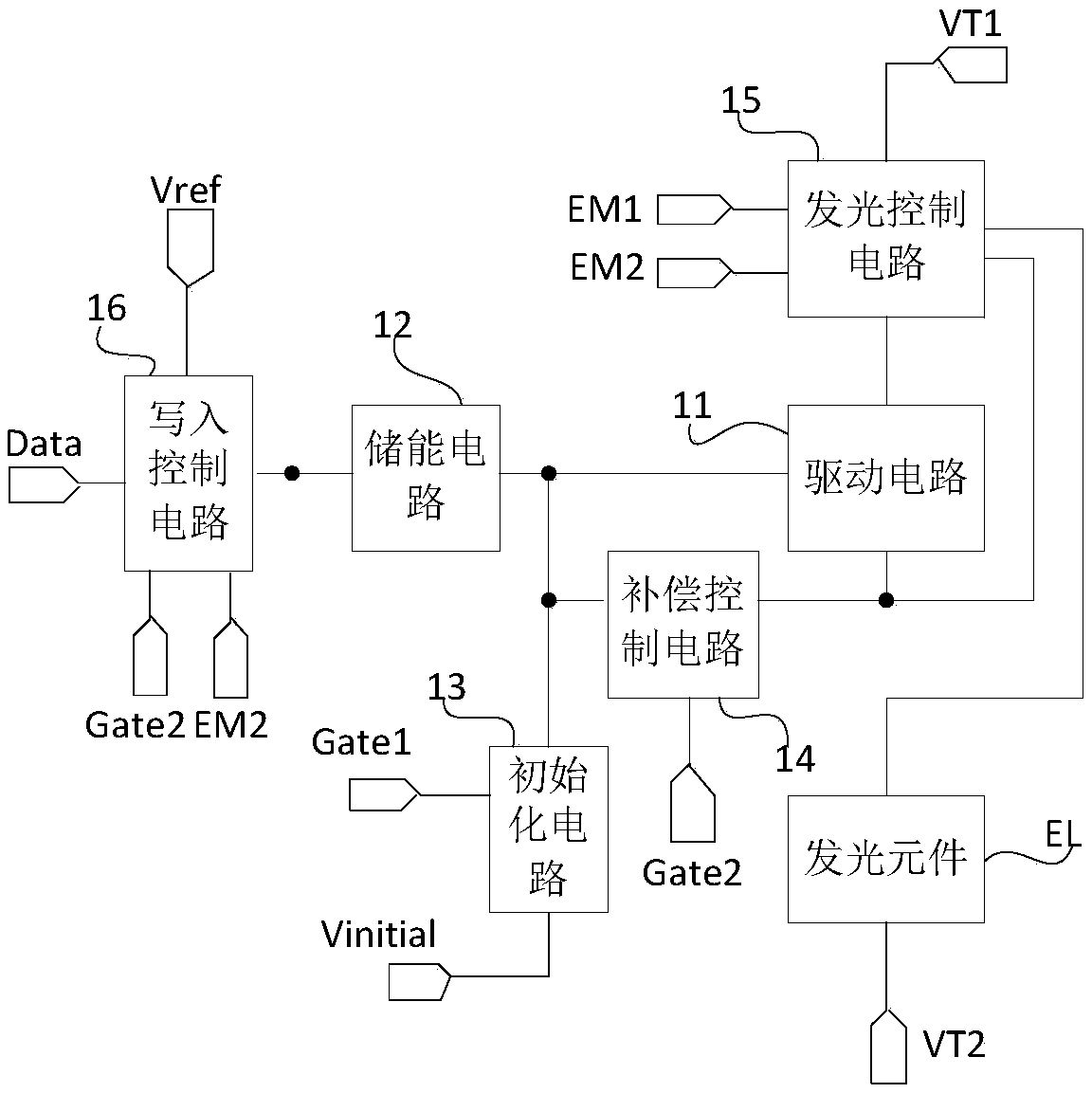
[0003] The main purpose of the present invention is to provide a pixel circuit, a pixel driving method and a display device to solve the problem in the prior art that the threshold voltage compensation cannot be performed while effectively improving short-term afterimages

Method used


Image

  • Pixel circuit, pixel driving method and display device
  • Pixel circuit, pixel driving method and display device
  • Pixel circuit, pixel driving method and display device

Examples


specific Embodiment approach

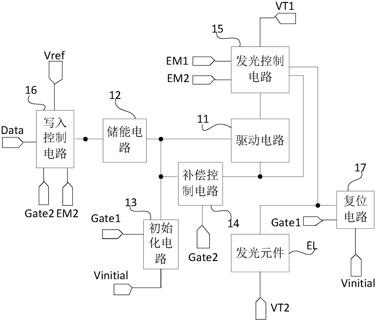
[0145] According to a specific implementation manner, the pixel circuit may further include a reset circuit; the pixel driving method further includes:

[0146] In the initialization phase, under the control of the first gate drive signal output by the first gate line, the reset circuit writes an initialization voltage into the first electrode of the light emitting element, so that the light emitting element does not to emit light, so that the charge remaining on the first electrode of the light-emitting element will not affect the display.

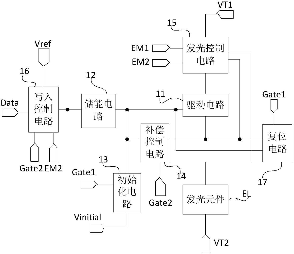
[0147] According to another specific implementation manner, the pixel circuit may further include a reset circuit; the pixel driving method may further include:

[0148] In the initialization phase, the reset circuit controls the communication between the control terminal of the driving circuit and the second terminal of the driving circuit under the control of the first gate driving signal output by the first gate line, Under the contro...

Embodiment approach

[0156] According to another specific implementation manner, the display device of the present invention further includes a gate driving circuit;

[0157] The gate drive circuit includes an N-level gate drive unit circuit;

[0158] The gate drive unit circuit at the nth stage is used to provide the first gate drive signal and the first light emission control signal for the pixel circuit in the nth row, and provide the second gate drive signal and the second gate drive signal for the pixel circuit in the n-1th row. The second lighting control signal, n is an integer greater than 1 but less than or equal to N;

[0159] The gate driving unit circuit in the first stage is used to provide the first gate driving signal and the first light emission control signal for the first row of pixel circuits.

[0160] In specific implementation, the first gate drive signal may be the same as the first light emission control signal, the second gate drive signal may be the same as the second lig...


PUM


Abstract

The invention provides a pixel circuit, a pixel driving method and a display device. The pixel circuit includes a light-emitting element, a driving circuit, an energy storage circuit, an initialization circuit, a compensation control circuit, a light-emitting control circuit and a writing control circuit. Under the control of a first gate driving signal, the initialization circuit writes initialization voltage to the control end of the driving circuit to control that the driving circuit to lead the connection between its first end and second end. Under the control of a second gate driving signal, the compensation control circuit controls and leads the connection between the control end of the driving circuit and the second end of the driving circuit. The problem is solved that the threshold voltage compensation can not be carried out when a short-term residual image is effectively improved in the prior art.

Description

technical field [0001] The present invention relates to the field of display technology, in particular to a pixel circuit, a pixel driving method and a display device. Background technique [0002] In the existing pixel circuit, since the threshold voltage shifts of the driving transistors are different, it is easy to cause unevenness in the entire display panel, so threshold voltage compensation is required. At the same time, due to the hysteresis effect of the driving transistor in the pixel circuit, existing OLED (Organic Light Emitting Diode) display products will find afterimages when switching to grayscale images after lighting up black and white images for a period of time, and then the afterimages will disappear after a period of time. It is short-term afterimage, and the existing technology cannot effectively improve the problem of short-term afterimage. Contents of the invention [0003] The main purpose of the present invention is to provide a pixel circuit, a ...

Claims


Application Information

Patent Timeline
IPC IPC(8): G09G3/3208
CPCG09G3/3208G09G3/325G09G3/3225G09G2300/0426G09G2300/0814G09G2300/0819G09G2300/0852G09G2300/0866G09G2320/045G09G3/3258G09G3/3291G09G3/32
Inventor 王志冲
Owner ORDOS YUANSHENG OPTOELECTRONICS
Learn More