Optical proximity correction method for optimizing connection performance of through hole layers

A technology of optical proximity correction and through-hole connection, which is applied in the direction of optics, photographic process of pattern surface, and originals for photomechanical processing, etc. It can solve the problems of compressing narrow process window graphic process width, etc., and achieve optimal connection performance , the effect of increasing the coverage area

Active Publication Date: 2019-03-19
SHANGHAI HUALI MICROELECTRONICS CORP
View PDF4 Cites 2 Cited by
  • Summary
  • Abstract
  • Description
  • Claims
  • Application Information

AI Technical Summary

Problems solved by technology

The traditional approach increases the coverage of the metal layer, but at the same time reduces the isolated pa

Method used


Image

  • Optical proximity correction method for optimizing connection performance of through hole layers
  • Optical proximity correction method for optimizing connection performance of through hole layers
  • Optical proximity correction method for optimizing connection performance of through hole layers

Examples


Embodiment Construction

[0037] The following will clearly and completely describe the technical solutions in the embodiments of the present invention with reference to the accompanying drawings in the embodiments of the present invention. Obviously, the described embodiments are only some, not all, embodiments of the present invention. Based on the embodiments of the present invention, all other embodiments obtained by persons of ordinary skill in the art without making creative efforts belong to the protection scope of the present invention.

[0038] It should be noted that, in the case of no conflict, the embodiments of the present invention and the features in the embodiments can be combined with each other.

[0039] The present invention will be further described below in conjunction with the accompanying drawings and specific embodiments, but not as a limitation of the present invention.

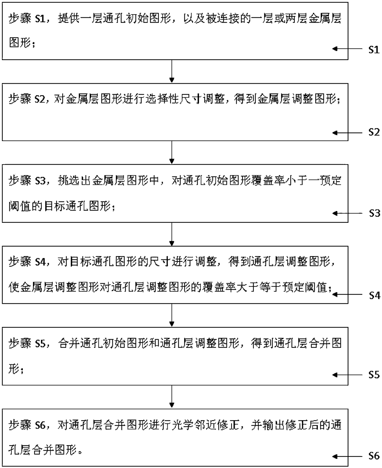
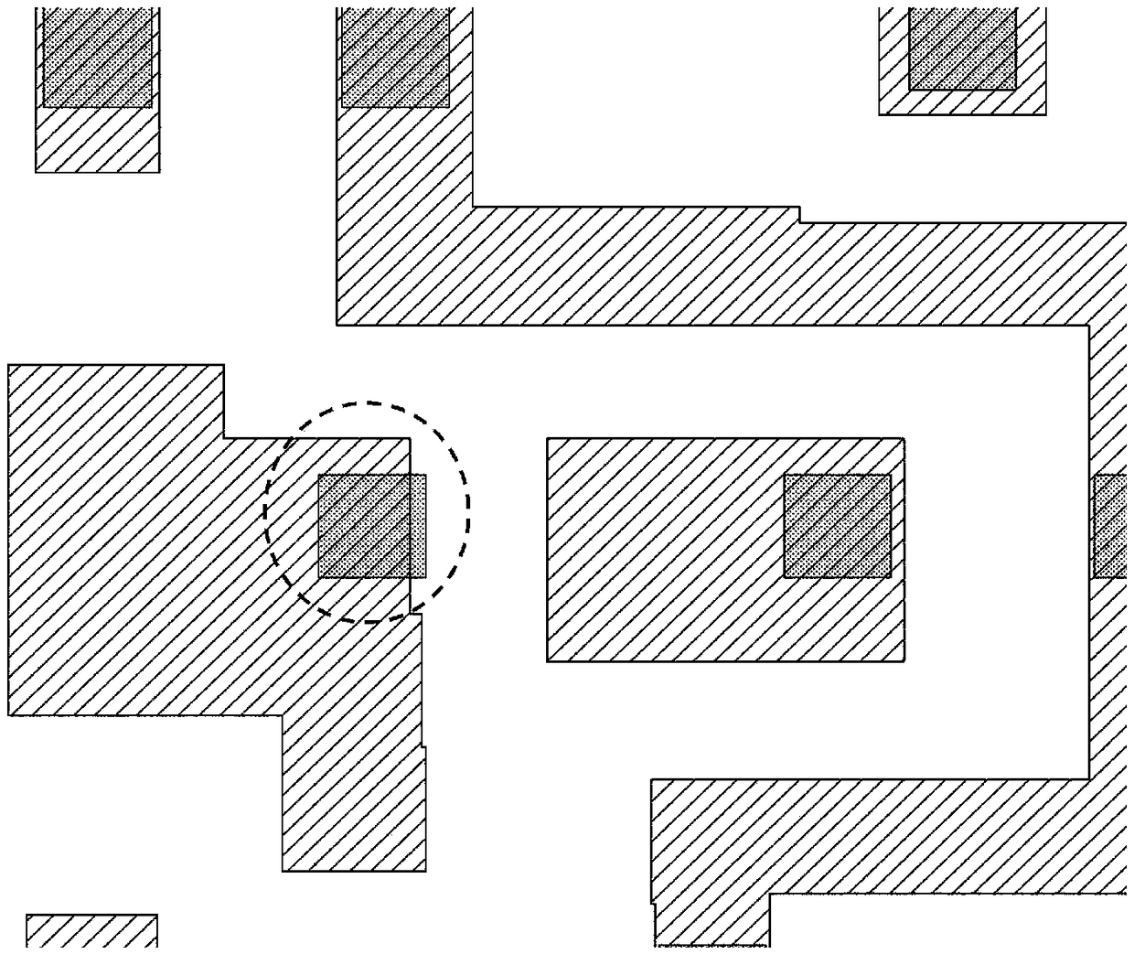
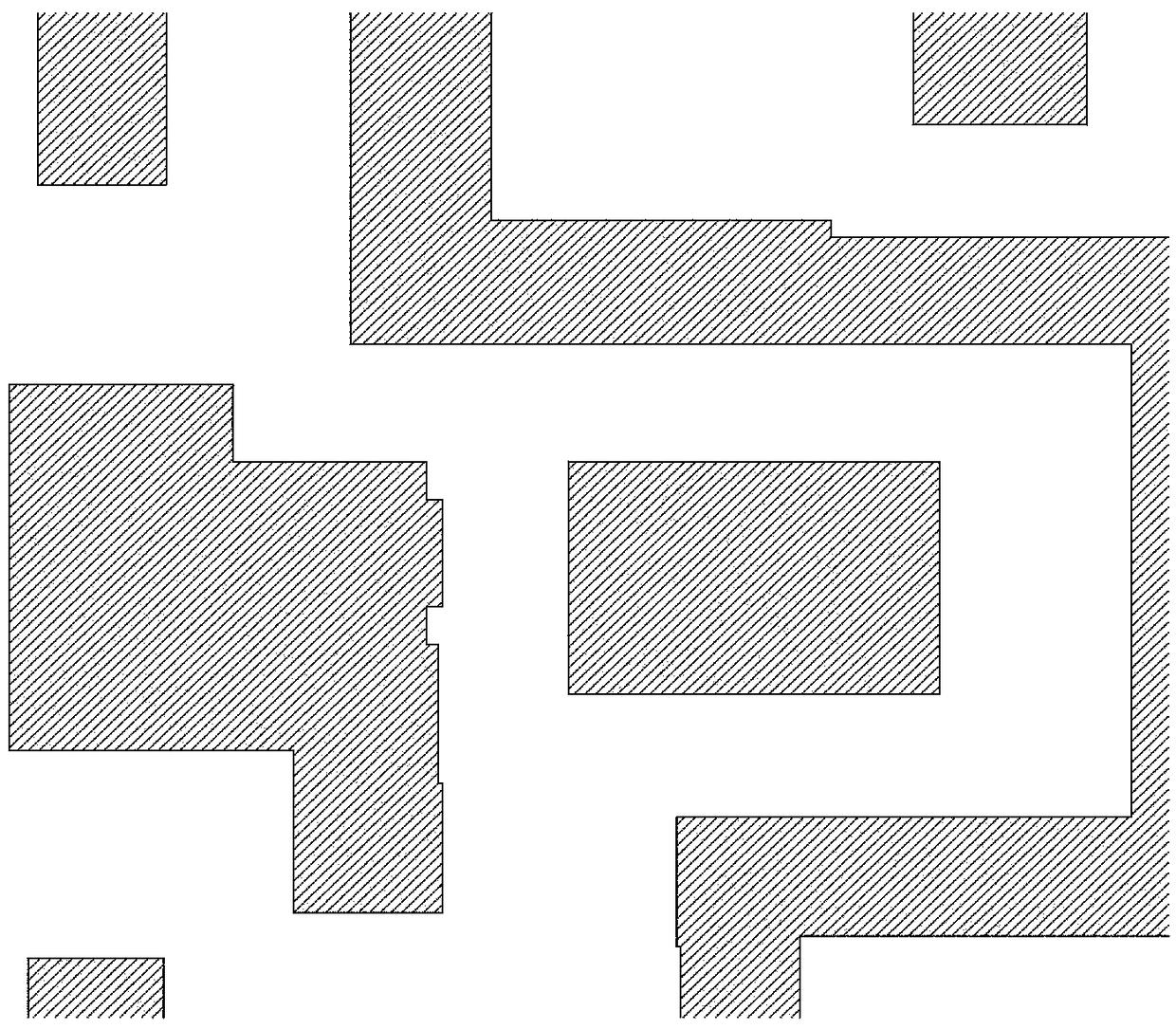
[0040] Based on the above-mentioned problems in the prior art, an optical proximity correction method for o...


PUM


Abstract

The invention discloses an optical proximity correction method for optimizing the connection performance of through holes. The method comprises the steps that S1 a through hole initial pattern and oneor two connected metal layer patterns are provided; S2 selective size adjustment is carried out on the metal layer pattern to acquire a metal layer adjusted pattern; S3 a target through hole patternwith the through hole initial pattern coverage less than a predetermined threshold is acquired; S4 the size of the target through hole pattern is adjusted to acquire a through hole layer adjusted pattern, so that the coverage of the metal layer adjusted pattern on the through hole layer adjusted pattern is greater than or equal to the predetermined threshold; S5 the through hole initial pattern and the through hole layer adjusted pattern are combined to acquire a through hole layer combined pattern; and S6 optical proximity correction is carried out on the through hole layer combined pattern,and the corrected through hole layer combined pattern is output. The method provided by the technical scheme of the invention can effectively make up for insufficient coverage caused by metal layer size adjustment and ensure the process width of a narrow process window pattern of a metal layer.

Description

technical field [0001] The invention relates to the technical field of integrated circuit photolithography technology, in particular to an optical proximity correction method for optimizing the connection performance of a via layer. Background technique [0002] In the back-end process manufacturing of integrated circuits, the effective connection between the metal layer and the via layer is an important factor to ensure product yield and performance. In an ideal design situation, the via pattern is completely contained within the metal pattern. However, in the actual process, the pattern of the metal layer on the silicon wafer will be affected by the optical proximity effect, resulting in deformation or distortion, and the connection of some via holes may be affected; in addition, with the continuous reduction of the line width, It is difficult to achieve a certain process window for all graphics under a certain process condition. In view of the above problems, by applyin...

Claims


Application Information

Patent Timeline
IPC IPC(8): H01L21/768G03F1/36
CPCG03F1/36H01L21/76838
Inventor 王靓莫保章
Owner SHANGHAI HUALI MICROELECTRONICS CORP
Why Eureka
Try Eureka