Circuit board electroplating process method

An electroplating process and circuit board technology, applied in the direction of electrical components, printed circuits, printed circuit manufacturing, etc., can solve the problems of different electroplating current density, uneven electroplating thickness, thick electroplating thickness, etc., achieve low implementation cost and improve uniform electroplating sexual effect

Active Publication Date: 2019-03-19
JCET GROUP CO LTD
View PDF19 Cites 3 Cited by
  • Summary
  • Abstract
  • Description
  • Claims
  • Application Information

AI Technical Summary

Problems solved by technology

[0002] With the diversification and miniaturization of electronic products, the precision of circuit boards is increasing day by day. When conventional plating lines are used, the plating current density is different due to the different distribution of plating lines on the circuit board. The thickness is thin, and the plating thickness is thick in the area with high current density, so it is easy to cause defects such as uneven plating thickness, seepage plating, and film clamping.
Circuit distribution generally has electrical requirements, which are difficult to optimize through design, and it is difficult to solve these problems only by improving the electroplating process capability, and the investment cost is relatively high

Method used


Image

  • Circuit board electroplating process method
  • Circuit board electroplating process method
  • Circuit board electroplating process method

Examples


Embodiment Construction

[0030] The present invention will be further described in detail below in conjunction with the accompanying drawings and embodiments.

[0031] A kind of circuit board electroplating process method in the present embodiment, it comprises the following steps:

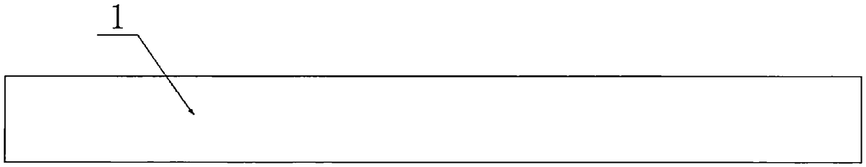
[0032] Step 1, see figure 1 , take a metal substrate, and the surface of the metal substrate is pre-plated with copper;

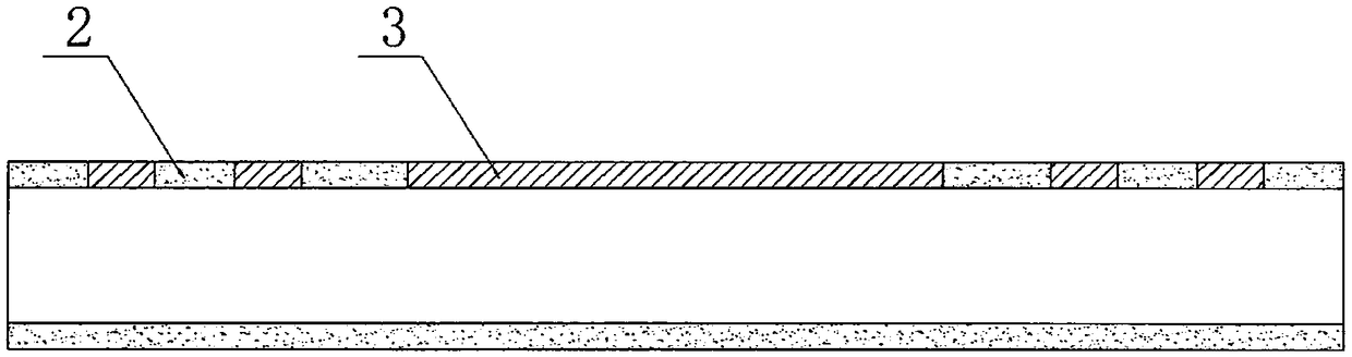
[0033] Step two, see figure 2 , coating the surface of the metal substrate with a photoresist film, exposing and developing the photoresist film, exposing the pattern area on the front of the metal substrate that needs to be electroplated, and forming the first circuit layer by electroplating on the pattern area;

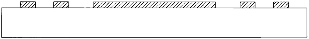
[0034] Step three, see image 3 , remove the photoresist film;

[0035] Step 4, see Figure 4 , press the ABF film on the front of the metal substrate, and perform heat curing operation, so that the first metal layer is covered in the cured ABF film;

[0036] Step five, see Figure ...


PUM


Abstract

The invention relates to a circuit board electroplating process method, which comprises the following steps: 1, a metal substrate is taken; 2, a first circuit layer is electroplated on the metal substrate; 3, an ABF film is pressed on the front surface of the metal substrate, and thermal curing operation is conducted to enable the first metal layer to be coated in the cured ABF film; 4, thinning is carried out to enable the first metal layer to expose the ABF film; 5, electroplating on the front surface of the metal substrate is carried out to form a second circuit layer, and electroplating onthe back surface of the metal substrate is carried out to form a compensation circuit layer; 7, the remaining photoresistive film is removed; and 8, window etching is carried out. According to the circuit board electroplating process method disclosed in the invention, the front electroplating thickness is optimized through a method of designing a compensation area on the back surface of a carrierplate, and the whole circuit electroplating uniformity is improved.

Description

technical field [0001] The invention relates to a circuit board electroplating process and belongs to the technical field of precision circuit boards. Background technique [0002] With the diversification and miniaturization of electronic products, the precision of circuit boards is increasing day by day. When conventional plating lines are used, the plating current density is different due to the different distribution of plating lines on the circuit board. The thickness is thin, and the plating thickness is thick in the area with high current density, so it is easy to cause defects such as uneven plating thickness, seepage plating, and film clamping. Circuit distribution generally has electrical requirements, which are difficult to optimize through design, and it is difficult to solve these problems only by improving the electroplating process capability, and the investment cost is relatively high. Contents of the invention [0003] The technical problem to be solved b...

Claims


Application Information

Patent Timeline
Patent Type & Authority Applications(China)
IPC IPC(8): H05K3/18H05K3/00
CPCH05K3/0005H05K3/18
Inventor 吴昊平张江华
Owner JCET GROUP CO LTD
Why Eureka
Try Eureka