
A kind of preparation method and device of high-quality silicon carbide crystal

A silicon carbide, high-quality technology, applied in chemical instruments and methods, crystal growth, single crystal growth, etc., can solve problems such as excessive carbonization rate, increased crystal stress, corrosion of crucible and insulation layer, etc., to avoid defects or cracks , reduce the risk of cracking, and stabilize the growth rate

Active Publication Date: 2020-08-07
SICC CO LTD
View PDF2 Cites 0 Cited by
  • Summary
  • Abstract
  • Description
  • Claims
  • Application Information

AI Technical Summary

Problems solved by technology

The problem of this invention is that, through the complicated preparation process, the second boost in the crystal growth stage makes the carbonization rate of silicon carbide powder difficult to control, the carbonization rate is too fast, the silicon component sublimates too fast and easily overflows, corrodes the crucible and heat preservation layer, and changing temperature and pressure can also lead to increased crystal stress, increasing the risk of crystal cracking

Method used


Image

  • A kind of preparation method and device of high-quality silicon carbide crystal
  • A kind of preparation method and device of high-quality silicon carbide crystal
  • A kind of preparation method and device of high-quality silicon carbide crystal

Examples


Embodiment approach

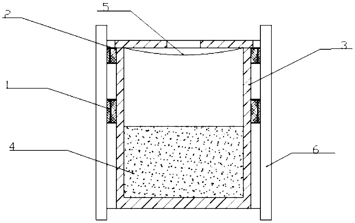
[0035]As an embodiment of the targeted design of the specific thermal field in the present invention: the first collar can reduce the temperature at the place where the seed crystal is placed; the second collar can increase the temperature on the surface of the raw material to form a specific thermal field area and change the temperature inside the crucible. The gas phase transmission path realizes fast and effective thermal field and fluid control.

[0036] Wherein, the projection height of the first collar to the graphite crucible is 25-35mm, preferably 28-32mm; the thickness of the first collar is 4-8mm, preferably 5-7mm. The first collar includes a graphite ring coated with a metal coating, the metal having a higher thermal conductivity than the graphite. Wherein, the thickness of the metal coating is 1-3 mm, preferably 2 mm.

[0037] in such as figure 1 In the shown embodiment, the first collar is a metal-coated graphite ring 1 whose bottom is substantially flat with th...

Embodiment 1

[0054] S1, put 6kg of silicon carbide powder into a graphite crucible, cover the crucible top cover with silicon carbide seed crystals, place a molybdenum-coated graphite ring and a zirconia-coated graphite ring in sequence on the outer wall of the graphite crucible, wherein the molybdenum-coated The layered graphite ring is placed on the surface of the silicon carbide powder, the zirconia-coated graphite ring is placed on the surface of the silicon carbide seed crystal, and then the insulation layer is wrapped, and the crystal growth furnace is sealed;

[0055] S2, evacuate the crystal growth furnace, pass helium gas protection for 5 hours, first raise the pressure to 10mbar at a rate of 2mbar / h, and then raise the temperature to 2400°C within 15h at a rate of 2.5°C / min;

[0056] S3, under the conditions of 10mbar and 2400°C, crystal growth at constant temperature and pressure, and the growth time is 200h;

[0057] S4, the temperature is lowered and cooled for 20 hours, and t...

Embodiment 2

[0059] S1, put 6kg of silicon carbide powder into the graphite crucible, cover the crucible top cover with silicon carbide seed crystals, and place a tantalum-coated graphite ring and a zirconia-coated graphite ring in sequence on the outer wall of the graphite crucible, wherein the tantalum-coated The layered graphite ring is placed on the surface of the silicon carbide powder, the zirconia-coated graphite ring is placed on the surface of the silicon carbide seed crystal, and then the insulation layer is wrapped, and the crystal growth furnace is sealed;

[0060] S2, evacuate the crystal growth furnace, pass in neon gas for protection for 7 hours, first increase the pressure to 12mbar at a rate of 1mbar / h, and then increase the temperature to 2350°C within 14h at a rate of 3°C / min;

[0061] S3, under the conditions of 12mbar and 2350°C, crystal growth at constant temperature and pressure, and the growth time is 210h;

[0062] S4, the temperature was lowered and cooled for 18 ...


PUM

PropertyMeasurementUnit
thicknessaaaaaaaaaa
thicknessaaaaaaaaaa
heightaaaaaaaaaa

Abstract

The invention provides a method for preparing a high-quality silicon carbide crystal and a device thereof. The method comprises the steps of thermal field assembly, heating, crystal growing and cooling, wherein the step of thermal field assembly comprises the steps of putting a crystal growing raw material and silicon carbide seed crystal into a graphite crucible, setting a first lantern ring withthe heat conductivity greater than that of graphite on the outer wall of the graphite crucible roughly corresponding to the crystal growing material, and setting a second lantern ring with the heat conductivity less than that of graphite roughly corresponding to the silicon carbide seed crystal. The invention further provides a device for implementing the method. According to the preparation method and device of the silicon carbide crystal, introduction of other component or complicated preparation process is not required, carbon inclusion defect is prevented by controlling the thermal fieldin the crystal growing furnace, the risk of cracking crystal can be reduced, and the quality of silicon carbide crystal can be improved.

Description

technical field [0001] The invention relates to the technical field of crystal growth, in particular to a method for preparing high-quality silicon carbide crystals and a device thereof. Background technique [0002] Silicon carbide (SiC) single crystal material is a representative of the third generation of wide bandgap semiconductor materials, with properties such as wide bandgap, high thermal conductivity, high electron saturation migration rate, high breakdown electric field, etc. Ideal semiconductor materials for high-power devices and high-temperature electronic devices. The physical vapor transport (PVT) method is a widely used technology for growing SiC single crystals. SiC wafers are used as seed crystals, and SiC powder is installed in graphite crucibles as growth materials. The silicon carbide powder is decomposed and sublimated into gas phase components. The gas phase components move to the growth interface with relatively low temperature, and crystallize on th...

Claims


Application Information

Patent Timeline
Patent Type & Authority Patents(China)
IPC IPC(8): C30B29/36C30B23/00
CPCC30B23/00C30B29/36
Inventor 李长进李加林李宏刚刘家朋孙元行刘鹏飞高超宗艳民
Owner SICC CO LTD
Learn More