Semiconductor device and semiconductor device manufacturing method

Inactive Publication Date: 2007-06-07
FUJITSU MICROELECTRONICS LTD
View PDF9 Cites 32 Cited by
  • Summary
  • Abstract
  • Description
  • Claims
  • Application Information

AI Technical Summary

Benefits of technology

[0011] the first field effect type transistor comprising a first gate electrode, a first insulating layer under the first gate electrode, a conductive layer of the second conductivity type for forming a first conductive path of the first conductivity type under the first insulating layer, a first conductivity type originating area that is formed at one end of a second conductivity type area which should become the first conductive path, and that should become an originating point of the first conductive path, and a first conductivity type terminating area that is formed at the other end of the second conductivity type area and that should become a terminating point of the first conductive path, the second field effect type transistor comprising a second gate electrode, a second insulating layer under the second gate electrode, a conductive layer of the first conductivity type for forming a second conductive path of the second conductivity type under the second insulating layer, a second conductivity type originating area that is formed at one end of a first conductivity type area which should become the second conductive path, and that should become an originating point of the second conductive path, and a second c

Problems solved by technology

Due to such a separate use of these stresses, however, the attachment of the different types of films to the surfaces of the NMOS transistor portion and the PMOS transistor portion of the CMOS semi

Method used


Image

  • Semiconductor device and semiconductor device manufacturing method
  • Semiconductor device and semiconductor device manufacturing method
  • Semiconductor device and semiconductor device manufacturing method

Examples


first embodiment

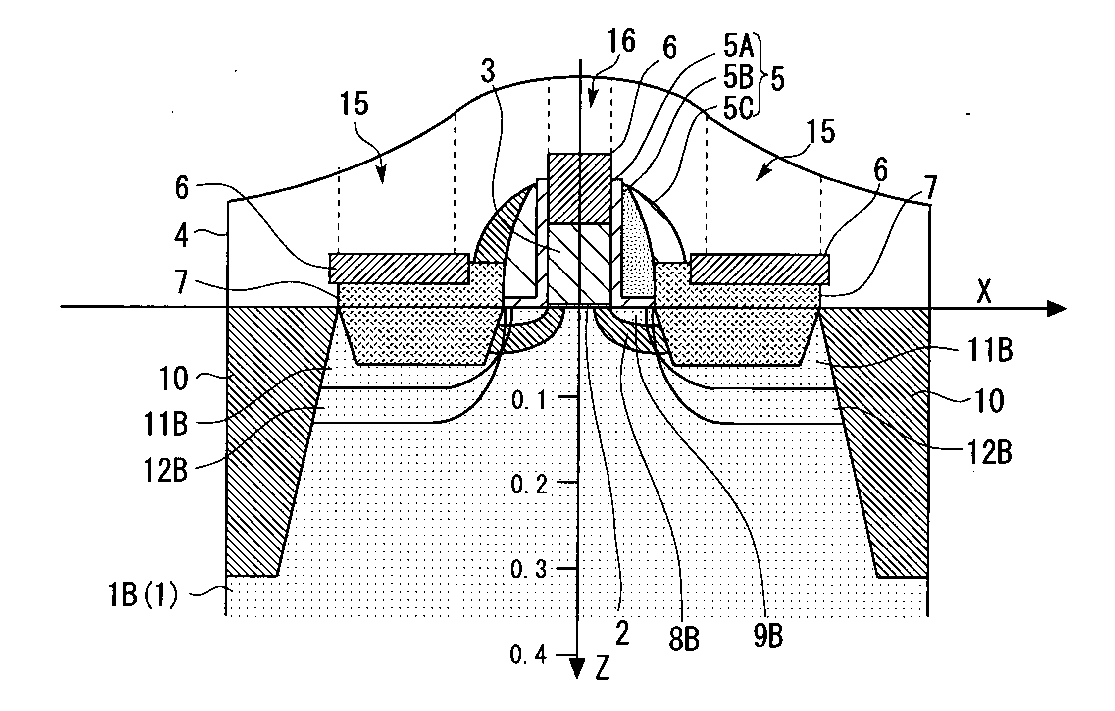
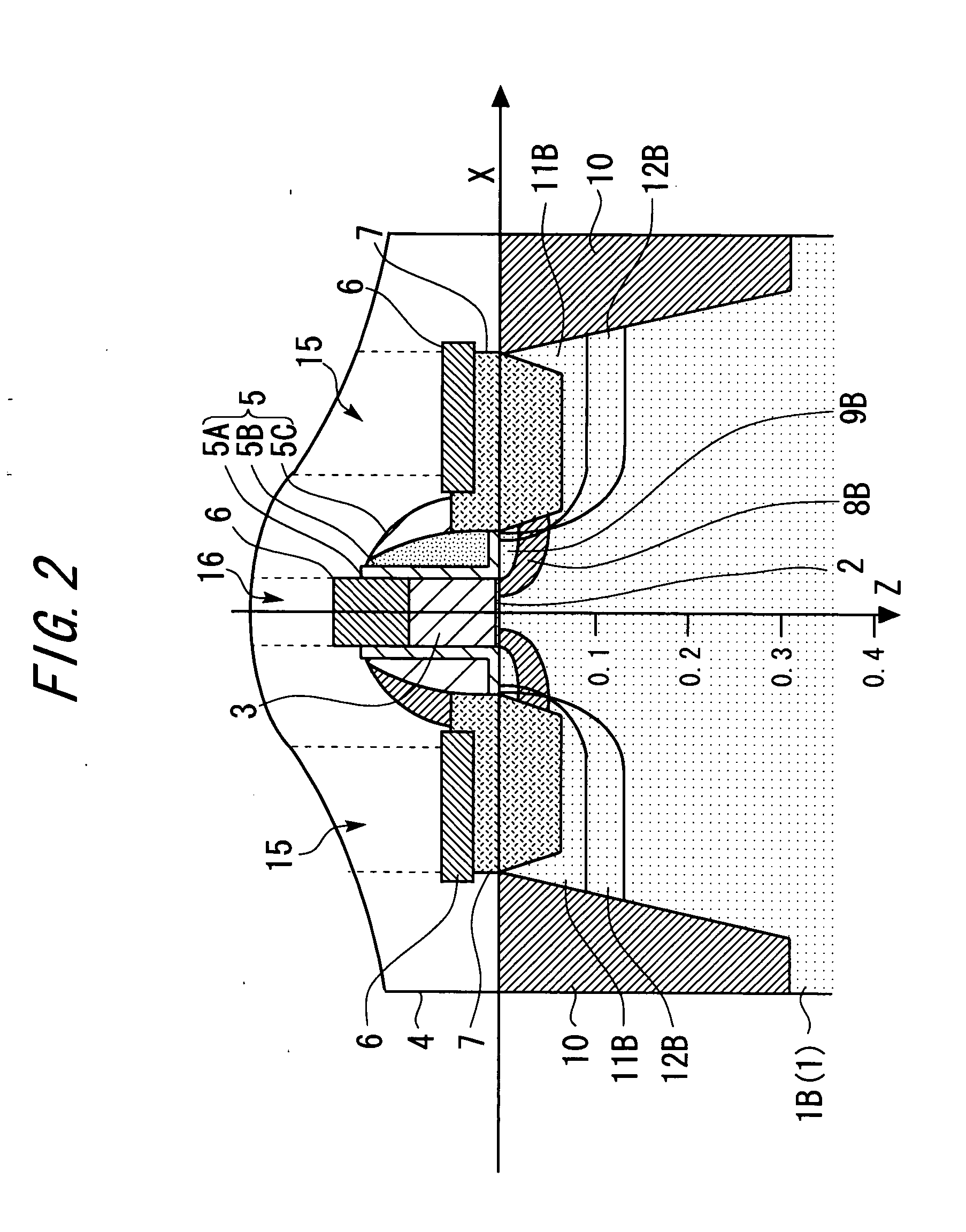
[0061] Next, the gate 3 is formed of, e.g., polysilicon(polycrystalline silicon) by a known process on the semiconductor substrate 1. Herein, for example, after the polysilicon has been formed (deposited) on the substrate surface by the CVD method etc, a photoresist is coated, and the photoresist excluding the area of the gate 3 is removed. Then, the area of the gate 3 is protected by the photoresist, and an area other than the area of the gate 3 is etched. In the first embodiment, at this point of time the film thickness of the gate 3 is on the order of 100 nm.

[0062] Next, as shown in FIG. 5A, an N-type extension layer 9A and a P-type pocket layer 8A are formed in the NMOS transistor portion (the P-well 1A portion). The N-type extension layer 9A is formed by implanting, e.g., an impurity such as arsenic (or phosphorous) (herein, the arsenic is used with an energy of 1.0 Kev and with a dose of 1×10¹⁵). Further, the P-type pocket layer 8A is formed by implanting the impurity such as ...

second embodiment

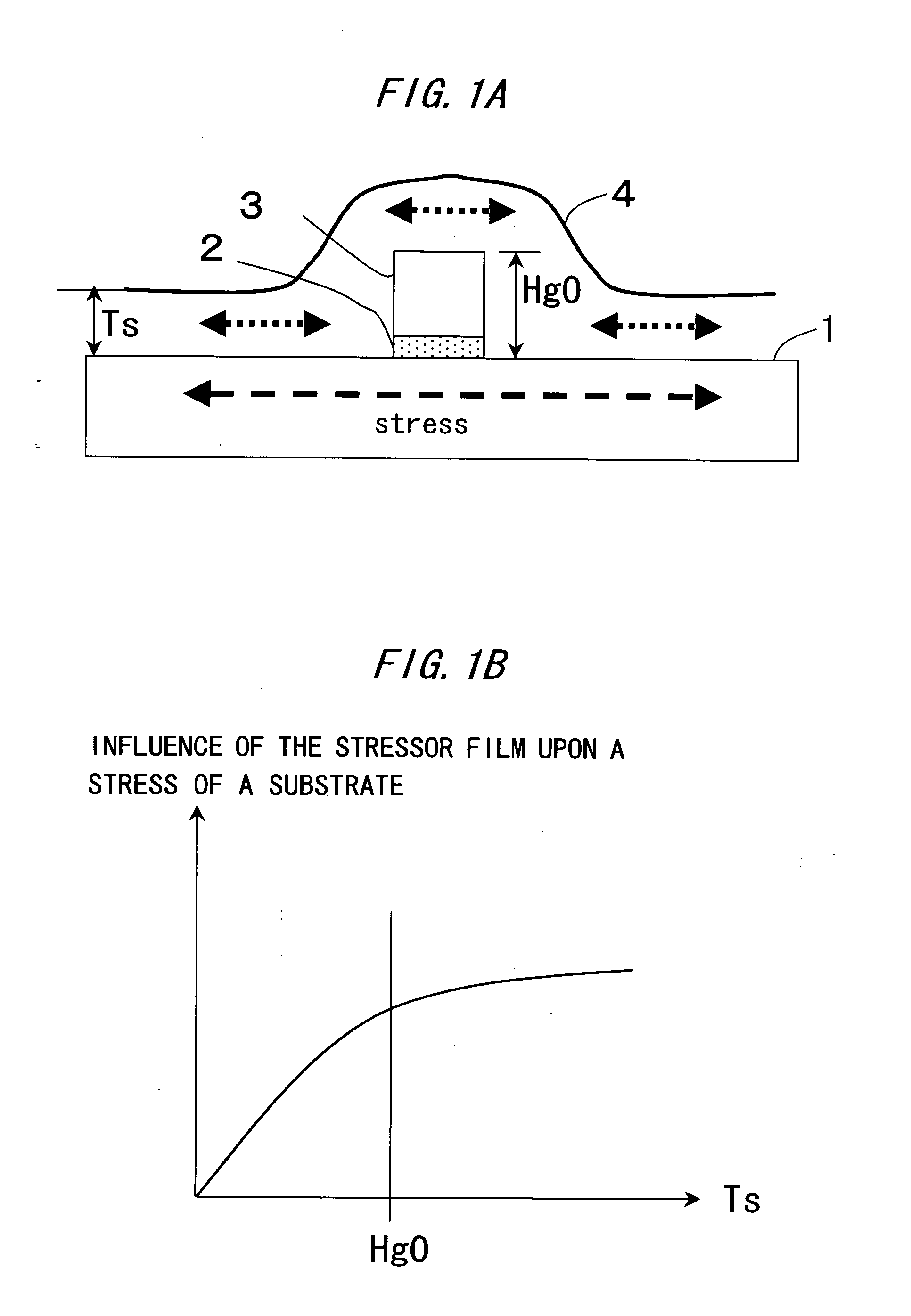
[0099] As discussed above, according to the semiconductor device in the second embodiment, in the case where the film with the tensile stress occurred is formed as the stressor film 4, the electron mobility in the NMOS transistor can be improved. Further, the influence by the stressor film 4 upon the PMOS transistor is reduced by decreasing the height of the gate 3B of the PMOS transistor, whereby the tensile stress can be reduced. Accordingly, the decrease in the hole mobility of the PMOS transistor can be restrained.

[0100] The second embodiment has dealt with the semiconductor device in which the film with the tensile stress occurred is formed as the stressor film 4 by decreasing the height of the gate 3B of the PMOS transistor. The second embodiment has dealt specifically with the semiconductor device having none of the stressor portion in the recessed portion 14 in the area of the P-type first source / drain 11B. As a substitute for this configuration, there may be configured a se...


PUM


Abstract

A semiconductor device is configured so that there is formed a stressor film 4 covering the first field effect transistor and the second field effect transistor, formed with openings from which the originating area and the terminating area of each of the first field effect transistor and the second field effect transistor are partially exposed, and applying a stress to at least an area extending from the vicinity of the originating area to the vicinity of the terminating area of each of the first field effect transistor and the second field effect transistor, and that a height of a first gate electrode 3 (3A) in a direction substantially perpendicular to a first insulating layer is set different from a height of a second electrode 3 (3B) in the direction substantially perpendicular to a second insulating layer.

Description

BACKGROUND OF THE INVENTION [0001] The invention relates to a CMOS semiconductor device. [0002] A variety of proposals (refer to Patent documents 1 through 3) are made in order to increase a process margin when manufacturing a semiconductor device or to improve an electric characteristic of the semiconductor device. [0003] Especially, recognition acquired over the recent years is that element performance is changed by applying a stress to a semiconductor device. It is generally known that an NMOS semiconductor device gets improvement of an electron mobility due to a stress acting in a direction of stretching (a direction in which an interval between atoms structuring a crystal expands) within a plane parallel with a substrate of the semiconductor device. On the other hand, it is known that a PMOS semiconductor device gets improvement of a hole mobility due to a stress acting in a direction of compressing (a direction in which the interval between atoms structuring the crystal shrink...

Claims


Application Information

Patent Timeline
IPC IPC(8): H01L29/76
CPCH01L29/165H01L29/665H01L29/66545H01L29/6656H01L29/6659H01L29/66628H01L29/66636H01L29/7834H01L29/7843H01L29/7848
Inventor OHTA, HIROYUKIHATADA, AKIYOSHISHIMAMUNE, YOSUKEKATAKAMI, AKIRATAMURA, NAOYOSHI
Owner FUJITSU MICROELECTRONICS LTD
Why Eureka
Try Eureka