A method of measuring bond strength

A bonding strength and bonding technology, which is applied to measuring devices, instruments, and mechanical devices, can solve problems such as inaccurate measurement of the gap length L and inaccurate calculation of bonding strength, and achieve simple and effective measurement and improve accuracy Effect

Active Publication Date: 2021-10-01
SHANGHAI HUALI MICROELECTRONICS CORP
View PDF2 Cites 0 Cited by
  • Summary
  • Abstract
  • Description
  • Claims
  • Application Information

AI Technical Summary

Problems solved by technology

[0017] However, in the BSI process, there is metal copper on the bonded wafer, and IR is difficult to penetrate, which leads to inaccurate measurement of the gap length L, which leads to inaccurate calculation of the bonding strength

Method used


Image

  • A method of measuring bond strength
  • A method of measuring bond strength
  • A method of measuring bond strength

Examples


Embodiment Construction

[0086] It should be noted that, in the case of no conflict, the following technical solutions and technical features can be combined with each other.

[0087] The specific embodiment of the present invention will be further described below in conjunction with accompanying drawing:

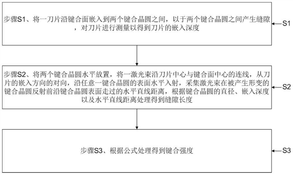
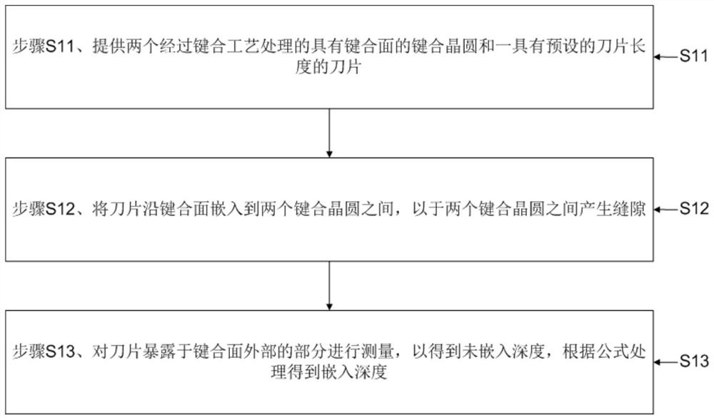
[0088] Such as Figure 2-5 As shown, a method for measuring the bonding strength is suitable for measuring the bonding strength between two bonded wafers. There is a bonding surface between the two bonded wafers, which can realize accurate measurement of the gap length. A convenient method for calculating bond strength includes the following specific steps:

[0089] Step S1, embedding a blade between two bonded wafers along the bonding surface to create a gap between the two bonded wafers, and measuring the blade to obtain the embedding depth of the blade;

[0090] Step S2, placing two bonded wafers horizontally, and injecting a laser beam horizontally along the line connecting the center of the ...


PUM


Abstract

The invention provides a method for measuring bonding strength, which belongs to the technical field of semiconductor manufacturing, comprising: embedding a blade between two bonding wafers along the bonding surface, so as to generate a gap between the two bonding wafers , measure the blade to get the embedding depth of the blade; place two bonded wafers horizontally, place a laser beam along the line connecting the center of the blade and the center of the bonding surface, from the direction opposite to the embedding direction of the blade, along any The surface of the bonded wafer is horizontally incident, and the horizontal straight-line distance traveled by the laser beam before being reflected by the deformed bonded wafer is collected, and processed according to the diameter, embedding depth and horizontal straight-line distance of the bonded wafer The length of the gap is obtained; the bond strength is obtained by processing according to the formula. The beneficial effect of the present invention is that it can solve the problem of measuring the bond strength of graphic chips (such as graphic chips with metal wiring) that cannot penetrate or have poor penetration ability of IR, can perform simple and effective measurement, and can improve the accuracy of measurement.

Description

technical field [0001] The invention relates to the technical field of semiconductor manufacturing, in particular to a method for measuring bonding strength. Background technique [0002] In the back-illuminated sensor (Back Side Illumination, BSI) process, two wafers need to be bonded together, and the weak bonding force (Van der Waals force) at room temperature is converted into strength by high-temperature annealing during bonding. Higher forms of covalent bonds, this process is called bonding (bonding). [0003] The bonding strength (bond strength) after bonding can be measured by an infrared (Infrared Radiation, IR) penetration method. Such as figure 1 As shown, when measuring, firstly, insert the blade into the two wafers that have been bonded (defined as figure 1 The upper wafer is the first wafer, and the lower wafer is the second wafer), so that a gap is formed between the two wafers, and then, the infrared device is used to measure the gap length L through IR pe...

Claims


Application Information

Patent Timeline
Patent Type & Authority Patents(China)
IPC IPC(8): G01N19/04G01B11/02
CPCG01B11/02G01N19/04
Inventor 曹玉荣李虎张志刚
Owner SHANGHAI HUALI MICROELECTRONICS CORP
Why Eureka
Try Eureka