Optical fingerprint module, screen assembly and electronic device

A fingerprint module and optical technology, applied in computer parts, character and pattern recognition, instruments, etc., can solve the problems of the difference between the actual distance and the design value, affecting the collection of fingerprint optical signals, and the scrap of the module, so as to reduce the defect rate. , reduce the number of parts, reduce the effect of influencing factors

Inactive Publication Date: 2019-03-29
昆山丘钛生物识别科技有限公司
View PDF3 Cites 6 Cited by
  • Summary
  • Abstract
  • Description
  • Claims
  • Application Information

AI Technical Summary

Problems solved by technology

[0003] Since the principle of convex lens imaging is adopted, the distance between the lens and the chip is required to be a fixed value. If there is a discrepancy between the actual module production and the theoretical value, it will affect the fingerprint optical signal collection, which will seriously cause the module to be scrapped and unusable.
The accuracy of the distance between the lens and the chip is determined by the accumulation of the machining accuracy and installation accuracy of the components between the two. In the existing technical solutions, the accuracy of the distance between the lens and the chip includes: the bonding accuracy between the bracket and the circuit substrate , the processing accuracy of the bracket itself, the assembly accuracy of the bracket and the lens, the processing accuracy of the lens itself, the bonding accuracy between the chip and the circuit substrate, the thickness accuracy of the chip itself, the flatness of the circuit substrate, etc., all these factors affect the lens and the chip. Accuracy of the distance between these factors, the accumulation of these factors will eventually lead to a greater risk of a difference between the actual distance between the lens and the chip of the actually produced module and the design value

Method used


Image

  • Optical fingerprint module, screen assembly and electronic device
  • Optical fingerprint module, screen assembly and electronic device
  • Optical fingerprint module, screen assembly and electronic device

Examples


no. 1 example

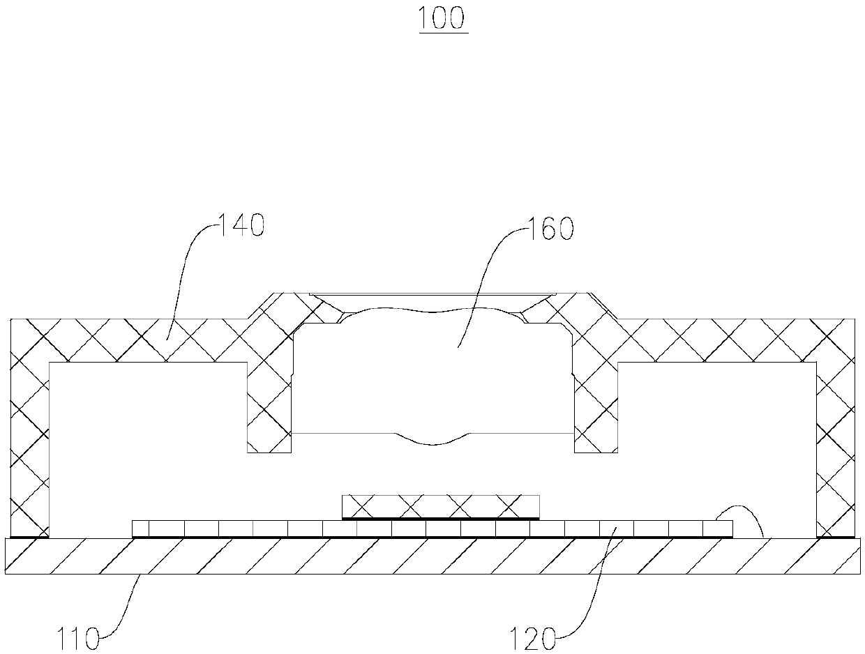
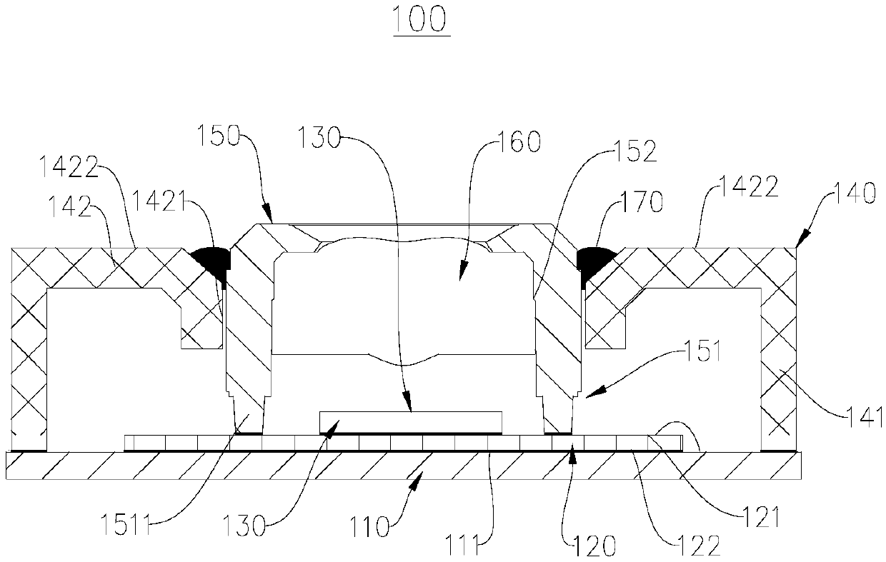
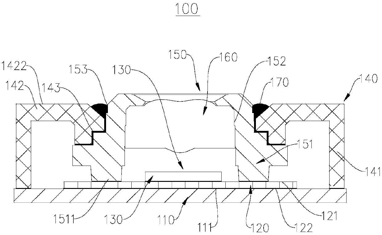
[0035]This embodiment provides an optical fingerprint module 100 to improve the actual distance between the lens 160 and the fingerprint identification chip 120 in the actual manufactured module that may occur in the existing optical fingerprint module 100 and the design value. big difference problem.

[0036] see figure 2 , the optical fingerprint module 100 includes a lens barrel 150 , a lens 160 , a filter 130 , a fingerprint identification chip 120 , a bracket 140 and a circuit substrate 110 .

[0037] The fingerprint identification chip 120 is arranged on the circuit substrate 110, the circuit substrate 110 includes a connection surface 111, the fingerprint identification chip 120 includes a first plane 121 and a second plane 122 opposite to the first plane 121, the first plane 121 of the fingerprint identification chip 120 Including the optical sensing area and the non-optical reaction area, the optical sensing area is used to sense and identify the fingerprint light a...

no. 2 example

[0051] This embodiment provides a screen assembly 200 , the screen assembly 200 includes a display screen 210 and the optical fingerprint module 100 provided in the first embodiment, and the optical fingerprint module 100 is arranged under the display screen 210 .

[0052] Screen assembly 200 is applied to electronic equipment, see Figure 7 , the screen assembly 200 also includes a middle frame 220 and a shielding foam 230. The optical fingerprint module 100 is fixed under the middle frame 220 by adhesive bonding or screw locking. The middle frame 220 is generally used to support and protect the display screen. 210. A shielding foam 230 is used between the middle frame 220 and the display screen 210 to prevent external stray light from interfering with the fingerprint optical signal. The display screen 210 may be an OLED screen, but is not limited thereto, and may also be other display screens 210 with the same or similar functions.

[0053] In another implementation of thi...

no. 3 example

[0055] This embodiment provides an electronic device, and the electronic device provided by this embodiment includes the screen component 200 provided by the second embodiment.

[0056] To sum up, the present invention provides an optical fingerprint module, a screen component and an electronic device. The optical fingerprint module includes: a lens barrel, lenses and a fingerprint recognition chip, the fingerprint recognition chip includes a first plane, the lens barrel includes a connecting portion and a mounting portion away from the connecting portion, the lens is mounted on the The installation part, the connection part is arranged on the first plane of the fingerprint identification chip so that the distance between the lens and the fingerprint identification chip is a preset value. The lens is directly connected to the fingerprint identification chip through the lens barrel, which removes the connection between the lens and the fingerprint identification chip, such as t...


PUM


Abstract

The invention provides an optical fingerprint module, a screen assembly and an electronic device, which relate to the technical field of the fingerprint module. The optical fingerprint module comprises: a lens barrel, a lens, a light filter and a fingerprint identification chip. the fingerprint identification chip includes a first plane, The optical filter is arranged on the first plane, the lensbarrel comprises a connecting part and a mounting part remote from the connecting part, the lens is mounted on the mounting part, and the connecting part is arranged on the first plane of the fingerprint identification chip so that the distance between the lens and the fingerprint identification chip is a preset value. As that len is arranged in the len barrel and the lens barrel is directly connected with the fingerprint identification chip, the factors affect the distance between the fingerprint identification chip and the fingerprint identification chip are reduced, the precision of the optical fingerprint module can be effectively improved, and the defect rate of the product can be reduced.

Description

technical field [0001] The invention relates to the technical field of fingerprint modules, in particular to an optical fingerprint module, a screen component and electronic equipment. Background technique [0002] The existing optical fingerprint module consists of a bracket, a lens, a filter, a fingerprint chip, and a circuit substrate. The chip is fixed on the circuit substrate with glue, and the electrical signal connection is realized between the gold wire and the circuit substrate. The optical filter is bonded to the chip with optical glue, and the bracket is bonded to the circuit substrate with structural glue. , the lens assembly is fixed in the bracket hole, the lens is a convex lens imaging principle, and the fingerprint optical signal is focused on the chip sensing area to collect fingerprints. [0003] Since the principle of convex lens imaging is adopted, the distance between the lens and the chip is required to be a fixed value. If there is a discrepancy betwe...

Claims


Application Information

Patent Timeline
Patent Type & Authority Applications(China)
IPC IPC(8): G06K9/00G06K9/20
CPCG06V40/13G06V10/147
Inventor 邹兵韦习贵
Owner 昆山丘钛生物识别科技有限公司
Why Eureka
Try Eureka