Solid-state image sensor and imaging device using same

a technology of image sensor and image sensor, which is applied in the direction of optical radiation measurement, radiation control device, instruments, etc., can solve the problem of increasing the possibility of distance measurement error, and achieve the effect of high-quality distance measuremen

Inactive Publication Date: 2017-12-28
PANASONIC INTELLECTUAL PROPERTY MANAGEMENT CO LTD
View PDF5 Cites 5 Cited by
  • Summary
  • Abstract
  • Description
  • Claims
  • Application Information

AI Technical Summary

Benefits of technology

[0007]A case in which the solid-state imaging device in PTL 2 is used as a distance measuring sensor is assumed. For example, a subject is irradiated with infrared light and is captured for a predetermined exposure time period by the distance measuring camera. In such a way, signal charges generated by reflected light are obtained. Here, the speed of light is approximately 30 cm per 1 ns, and the infrared light returns from an object located apart from the distance measuring sensor by 1 m when approximately 7 ns elapses after the infrared light has been emitted, for example. Therefore, control of an exposure time period of an extremely short time, for example, 10 ns to 20 ns is important to obtain high distance accuracy.
[0009]An object of the present disclosure is to allow a solid-state image sensor provided with a photoelectric conversion part having the vertical overflow drain structure to be used as, for example, a distance measuring sensor with high accuracy.
[0011]According to this aspect, the impurity induced part into which impurity of the first conductive type is induced is formed below the connecting part that supplies the substrate discharge pulse signal to the semiconductor substrate. Therefore, in a path in which the substrate discharge pulse signal is transferred to the photoelectric conversion part through the inside of the semiconductor substrate, a resistance in a direction perpendicular to the surface of the substrate can be significantly reduced. With this configuration, waveform distortion and delay in the pulsed substrate-discharge signal that reaches the photoelectric conversion parts can be suppressed. Accordingly, when the solid-state image sensor is used as the distance measuring sensor, an amount of a signal generated by the reflected light can be measured correctly, and therefore an error contained in a measured distance can be reduced.
[0014]According to the present disclosure, waveform distortion and delay in the substrate discharge pulse signal that reaches the photoelectric conversion parts can be suppressed, and therefore the solid-state image sensor can be used as a highly accurate distance measuring sensor, for example.

Problems solved by technology

In other words, when waveform distortion or delay of a nanosecond order is produced in the substrate discharge pulse signal, signal charges generated by the reflected light cannot be obtained correctly, and therefore a possibility to cause an error in distance measurement is increased.

Method used


Image

  • Solid-state image sensor and imaging device using same
  • Solid-state image sensor and imaging device using same
  • Solid-state image sensor and imaging device using same

Examples


first exemplary embodiment

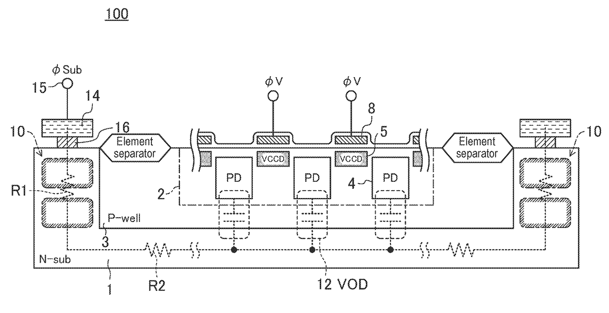
[0035]In a first exemplary embodiment, a solid-state image sensor is assumed to be a charge-coupled device (CCD) image sensor. Here, an interline transfer type CCD that corresponds to full pixel reading (progressive scan) will be described as an example.

[0036]FIG. 1 is a schematic sectional view illustrating a configuration of solid-state image sensor 100 according to the first exemplary embodiment. Illustration of components that do not directly relate to the description of the present disclosure such as a microlens or an intermediate film disposed above a wiring layer is omitted for simplification of the description.

[0037]In the configuration illustrated in FIG. 1, semiconductor substrate 1 is a silicon substrate of an N-type as a first conductive type. Well region 3 of a P-type as a second conductive type (hereafter, referred to as P well region) is formed at a surface part of one surface of semiconductor substrate 1. In P well region 3, pixel array part 2 provided with photoelec...

second exemplary embodiment

[0064]In a second exemplary embodiment, the solid-state image sensor is assumed to be a complementary metal oxide semiconductor (CMOS) image sensor. However, an object of the second exemplary embodiment is to suppress waveform distortion and delay of φSub, which is the same as the object of the first exemplary embodiment. Here, a CMOS image sensor mounted with an analog-to-digital converter of a column parallel type will be described as an example. A sectional structure of the CMOS image sensor is identical to that of the first exemplary embodiment, and therefore a description of the sectional structure is omitted in the present exemplary embodiment.

[0065]FIG. 14 is a schematic plan view illustrating an example of a configuration of a solid-state image sensor according to the present exemplary embodiment. Solid-state image sensor 200 in FIG. 14 includes pixel array part 22, vertical signal lines 25, horizontal scanning line group 27, vertical scanning circuit 29, horizontal scanning...

third exemplary embodiment

[0074]In a third exemplary embodiment, a solid-state image sensor is the CCD image sensor similarly to the first exemplary embodiment, but a difference lies in a process for forming the N-type epitaxial layer formed on the semiconductor substrate. However, an object of the third exemplary embodiment is to suppress waveform distortion and delay of φSub, which is the same as the object of the first exemplary embodiment. Here, differences from the first exemplary embodiment will be mainly described.

[0075]Each of FIGS. 15A and 15B is a schematic sectional view illustrating examples of a configuration and a manufacturing process of the solid-state image sensor according to the present exemplary embodiment. As illustrated in FIG. 15B, in this solid-state imaging device, for example, photoelectric conversion parts 4 and inter-pixel separators 6 that separate photoelectric conversion parts 4 are formed over first epitaxial layer 400 and second epitaxial layer 500, which are the N-type, on s...


PUM


Abstract

A solid-state image sensor including photoelectric conversion parts having a vertical overflow drain structure is made usable as, for example, a distance measuring sensor with high accuracy. In the solid-state image sensor, a pixel array part is formed in a well region of a second conductive type formed at a surface part of a semiconductor substrate of a first conductive type. In the pixel array part, photoelectric conversion parts each of which converts incident light into signal charges and has the vertical overflow drain structure (VOD) are arranged in a matrix form. Substrate discharge pulse signal φSub for controlling potential of the VOD is applied to a signal terminal. An impurity induced part into which impurity of the first type is induced is formed below a connecting part in the semiconductor substrate.

Description

TECHNICAL FIELD[0001]The present disclosure relates to a solid-state image sensor used, for example, in a distance measuring camera.BACKGROUND ART[0002]PTL 1 discloses a distance measuring camera having a function for measuring a distance to a subject using infrared light. In general, a solid-state image sensor used in the distance measuring camera is referred to as a distance measuring sensor. Particularly, a camera that is mounted on a game machine and detects movement of a body or hands of a person who is the subject is also referred to as a motion camera.[0003]PTL 2 discloses a solid-state imaging device having a vertical transfer electrode structure that can simultaneously read all pixels. Specifically, the solid-state imaging device is a charge-coupled device (CCD) image sensor provided with a vertical transfer part extending in a vertical direction adjacent to each column of photo diodes (PD).[0004]The vertical transfer part includes four vertical transfer electrodes correspo...

Claims


Application Information

Patent Timeline
Patent Type & Authority Applications(United States)
IPC IPC(8): G01J1/42G01S7/486G01J1/44H04N5/378H01L27/148G01S7/4863G01S17/894
CPCG01J1/4228G01J1/44G01S7/486G01J2001/448H01L27/14875H04N5/378H01L27/14856G01S7/4863H01L27/14843H01L27/14887G01S17/894H04N25/622H04N25/75
Inventor ASANO, TAKUYASATO, YOSHINOBU
Owner PANASONIC INTELLECTUAL PROPERTY MANAGEMENT CO LTD
Why Eureka
Try Eureka