Method for forming conductive structure

A conductive structure and groove technology, which is applied in the manufacture of circuits, electrical components, semiconductors/solid-state devices, etc., can solve problems such as incomplete filling, easy formation of impurities or defects, and influence on the uniformity of conductive material growth. performance effect

Inactive Publication Date: 2019-03-29
WUHAN XINXIN SEMICON MFG CO LTD
View PDF7 Cites 0 Cited by
  • Summary
  • Abstract
  • Description
  • Claims
  • Application Information

AI Technical Summary

Problems solved by technology

[0003] However, during the preparation process of the existing conductive structure, impurities or defects are easily formed in the trenches, and the process of growing conductive materials is likely to be too concentrated at these impurities or defects, thereby affecting the un

Method used


Image

  • Method for forming conductive structure
  • Method for forming conductive structure
  • Method for forming conductive structure

Examples


Embodiment Construction

[0024] The present invention will be further described below in conjunction with the drawings and embodiments.

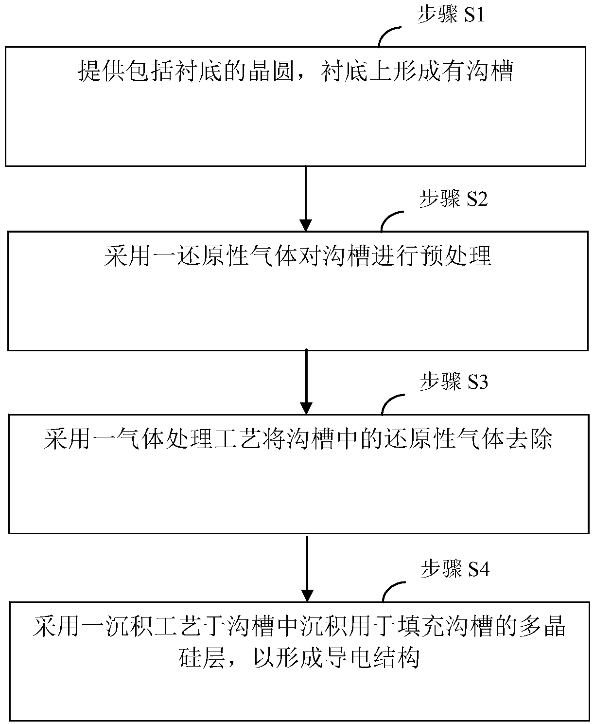
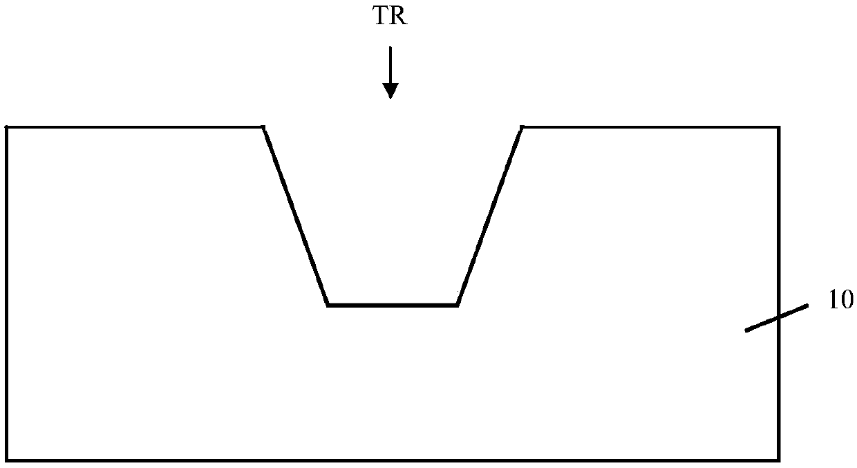
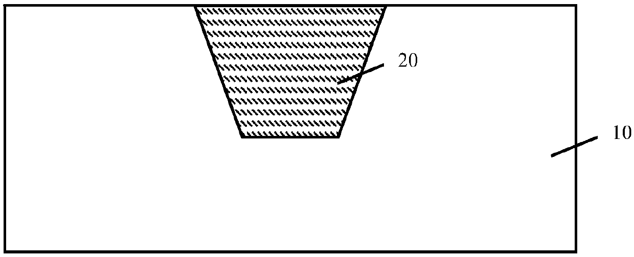
[0025] In a preferred embodiment, such as figure 1 As shown, a method for forming a conductive structure is proposed, and the formed structure can be as Figure 2~3 As shown, which can include:

[0026] Step S1, providing a wafer including a substrate 10 on which a trench TR is formed;

[0027] Step S2, pretreating the trench TR with a reducing gas;

[0028] Step S3, using a gas treatment process to remove the reducing gas in the trench TR;

[0029] Step S4, using a deposition process to deposit a polysilicon layer 20 for filling the trench TR in the trench TR to form a conductive structure.

[0030] In the above technical solution, the formed conductive structure may be a contact hole structure that electrically connects the top and bottom; other conventional structures for forming conductive structures may also be formed in the substrate 10 and in the trench TR, such as in t...


PUM


Abstract

The invention relates to the technical field of semiconductors, and especially relates to a method for forming a conductive structure. The method comprises the steps: S1, providing a wafer including asubstrate, wherein a groove is formed on the substrate; S2, pretreating the groove by using reducing gas; S3, using the gas processing process to remove the reducing gas in the groove; S4, employinga deposition process to deposit a polysilicon layer in the groove for filling the groove, so as to form a conductive structure. The conductive structure having a gap defect can be avoided, and the conductive structure is ensured to have excellent electrical properties.

Description

Technical field [0001] The present invention relates to the field of semiconductor technology, in particular to a method for forming a conductive structure. Background technique [0002] In semiconductor devices, such as flash memory devices, it is generally necessary to form a conductive structure for electrically connecting the upper and lower structures in the wafer. Such a conductive structure is generally formed in a trench, and the method of formation may be to fill the trench with a conductive material through a furnace tube. [0003] However, in the manufacturing process of the existing conductive structure, since impurities or defects are easily formed in the trench, the process of growing the conductive material tends to be too concentrated at these impurities or defects, thereby affecting the uniformity of the growth of the conductive material. In severe cases, it is easy to cause the conductive material to be sealed in the trench in advance, thereby forming incompletel...

Claims


Application Information

Patent Timeline
IPC IPC(8): H01L21/768
CPCH01L21/76814H01L21/76877
Inventor 徐杰
Owner WUHAN XINXIN SEMICON MFG CO LTD
Why Eureka
Try Eureka