
A serial port loading device and method for an embedded chip

An embedded chip, loading device technology, applied in the direction of instruments, electrical digital data processing, etc., can solve the problems that ROM is difficult to achieve universality, limited ROM space, poor reliability, etc., to save ROM storage space and GPIO resources, The effect of reducing hardware costs and labor costs, avoiding design difficulties and risks

Active Publication Date: 2019-04-02
上海移芯通信科技股份有限公司
View PDF6 Cites 3 Cited by
  • Summary
  • Abstract
  • Description
  • Claims
  • Application Information

AI Technical Summary

Problems solved by technology

[0003] In terms of programming function, ROM is difficult to achieve universality: 1. Since the technical standards of FLASH memories from different suppliers are not completely compatible, and the ROM space is limited, if the drivers required for the work of each FLASH memory are implemented one by one and Stored in the ROM, the ROM is programmed or booted through the driver, which will occupy a large storage space of the ROM; 2. The driver of various FLASH memories is very complicated to implement. If there is a slight error in the driver, after the chip tapes out Also because the driver program in the solidified storage space ROM cannot be changed, the driver program cannot work, and the chip cannot be burned and started, resulting in relatively serious economic losses
3. In NB-IOT SOC embedded chips, SPI NOR FLASH storage particles are often packaged inside the SOC embedded chip to reduce the overall space occupation of the SOC embedded chip. If the driver in the ROM is slightly defective, even if there are some SPI NOR FLASH can still work normally under such slight driver defects, but because SPINOR FLASH has been packaged inside the SOC, it is impossible to change such SPI NOR FLASH devices as easily as PCB circuits to achieve defect avoidance
[0004] In terms of programming efficiency: 1. Embedded chips are mostly programmed through the JLINK SWD interface. Although it is convenient for development and debugging, it is too dependent on JLINK hardware resources and KEIL tools, making automatic programming difficult; 2. Traditional Serial port programming requires humans to participate in operations such as reset, download, programming, and detection during the process. For example, when a reset is required, it is necessary to manually press the corresponding button to reset. In terms of mass production, the efficiency is low, the reliability is poor, and the cost high

Method used


Image

  • A serial port loading device and method for an embedded chip
  • A serial port loading device and method for an embedded chip
  • A serial port loading device and method for an embedded chip

Examples


Embodiment Construction

[0032] In order to more clearly illustrate the embodiments of the present invention or the technical solutions in the prior art, the specific implementation manners of the present invention will be described below with reference to the accompanying drawings. Obviously, the accompanying drawings in the following description are only some embodiments of the present invention, and those skilled in the art can obtain other accompanying drawings based on these drawings and obtain other implementations.

[0033] In order to make the drawing concise, each drawing only schematically shows the parts related to the present invention, and they do not represent the actual structure of the product. In addition, to make the drawings concise and easy to understand, in some drawings, only one of the components having the same structure or function is schematically shown, or only one of them is marked. Herein, "a" not only means "only one", but also means "more than one".

[0034]The embedde...


PUM


Abstract

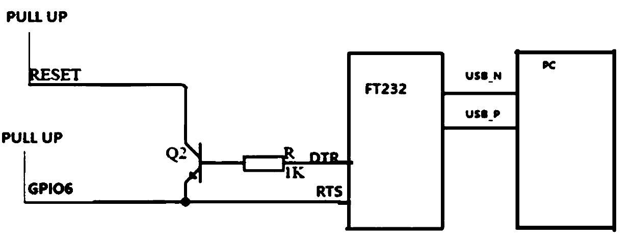
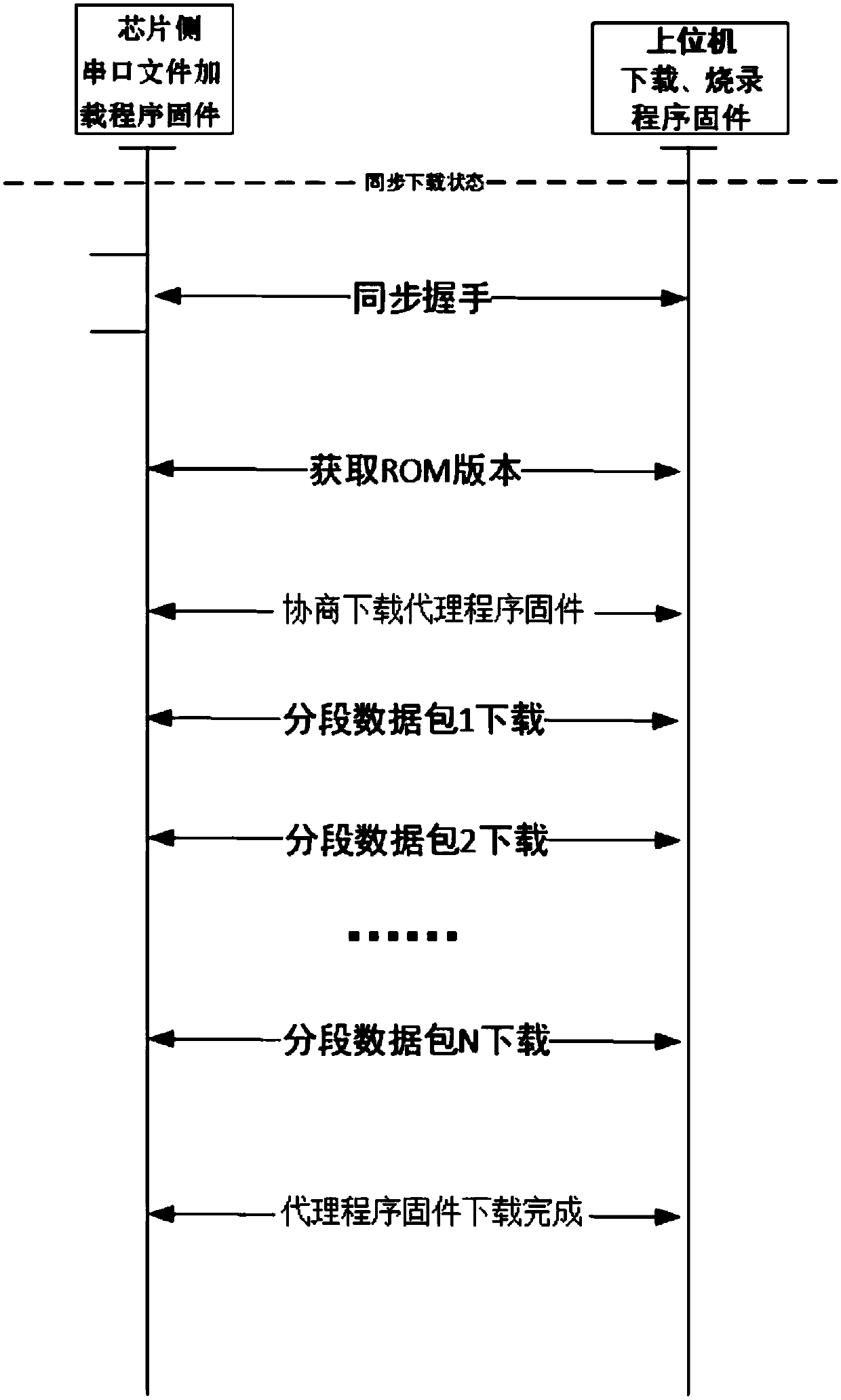
The invention discloses a serial port loading device and method for an embedded chip, and relates to the field of embedded chips, the serial port loading device comprises an embedded chip, a hardwarecontrol circuit, a USB conversion chip and an upper computer; and the embedded chip is in communication connection with the upper computer through the hardware control circuit and the USB conversion chip, so that the embedded chip and the upper computer realize serial port file loading. According to the invention, universal downloading and burning of the embedded chip are realized on the whole, the selection range of materials of the FLASH memory in the later stage is expanded, the ROM storage space and GPIO resources of the embedded chip are saved, and the design difficulty and risk of the ROM in the aspect of burning are avoided.

Description

technical field [0001] The invention relates to the field of embedded chips, in particular to a serial port loading device and method for embedded chips. Background technique [0002] Embedded chips refer to chips with ROM and RAM memory and control functions, such as SOC embedded chips. When a traditional embedded chip is started, it first needs to boot from the solidified storage space ROM inside the chip, and then further access other reprogrammable program storage media, such as SPI NOR FLASH in the FLASH memory, and jump to its corresponding image program space , so as to realize the functions of starting the program storage medium program and performing burning. [0003] In terms of programming function, ROM is difficult to achieve universality: 1. Since the technical standards of FLASH memories from different suppliers are not completely compatible, and the ROM space is limited, if the drivers required for the work of each FLASH memory are implemented one by one and ...

Claims


Application Information

Patent Timeline
Patent Type & Authority Applications(China)
IPC IPC(8): G06F13/40G06F13/42
CPCG06F13/4022G06F13/4282
Inventor 庄建伟常斌
Owner 上海移芯通信科技股份有限公司
Learn More