

Calibration structure design for on-chip load traction test of devices and test method
A load-pulling and testing method technology, applied in the direction of instruments, measuring devices, measuring electrical variables, etc., can solve the problems of inconsistent electrical characteristics, calibration errors, device testing accuracy, power amplifier design yield decline, etc., to improve testing accuracy, improve design The effect of yield
Inactive Publication Date: 2019-04-05
南京中电芯谷高频器件产业技术研究院有限公司
View PDF5 Cites 9 Cited by
- Summary
- Abstract
- Description
- Claims
- Application Information
AI Technical Summary
Problems solved by technology
[0004] However, there may be inconsistencies in the electrical characteristics between the calibration structure and the material and preparation process of the DUT, resulting in calibration errors, parasitic pads and interconnect lines, and a decline in device test accuracy and power amplifier design yield.
Method used
View moreImage
Smart ImageViewing Examples

Examples
Embodiment 1
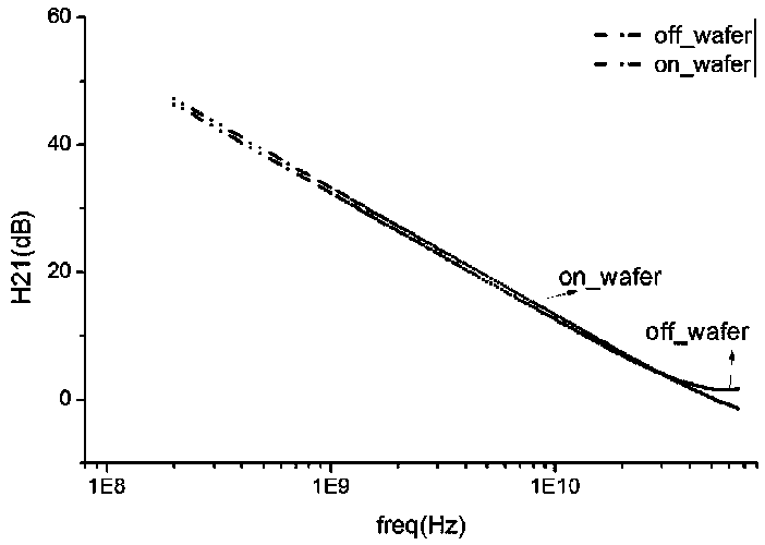
[0037] as attached image 3 As shown, the comparison results of small-signal data obtained by applying this method for calibration and using a commercial calibration sheet test, where On-wafer is the data obtained by applying this method for calibration, and off-wafer is the data obtained after using a commercial calibration sheet for calibration, as shown in the figure Using this method for calibration can effectively remove parasitic parameters and make test data more accurate.
Login to View More PUM
 Abstract
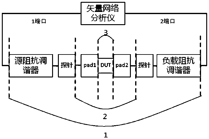
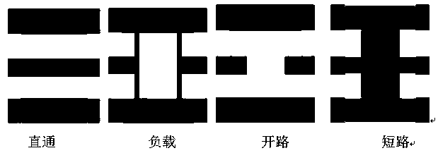
The invention relates to a calibration structure for on-chip load traction test of devices. The calibration structure comprises an open circuit part, a short circuit part, a load part and a through part, wherein the load part, the open circuit part, the short circuit part and the through part are completely consistent with a to-be-tested device bonding pad in the aspect of structure. The inventionfurthermore discloses a test method suitable for the on-chip load traction test of devices, and the method comprises the steps of: 1) calibrating dual ports of a vector network analyzer; 2) calibrating an impedance tuner and measuring a 1-port scattering parameter (S parameter) of the load; 3) inputting the parameter; 4) calibrating the end surfaces of a device; and 5) carrying out power calibration and verification. The calibration structure and the test method have the advantages of: 1) ensuring the consistent electric characteristics of the calibration structure and to-be-tested chips, soas to avoid calibration errors caused by inconsistent materials and preparation processes of the calibration structure and to-be-tested pieces; and 2) effectively stripping the bonding pad and interconnection line parasitism, so as to improve the device test precision and improve the power amplifier design yield.
Description
technical field [0001] The invention relates to a structural design and a testing method for device on-chip load pulling testing and calibration, and belongs to the technical field of semiconductor testing. Background technique [0002] With the rapid development of wireless communication and radar detection and other fields, power amplifiers and low-noise amplifier chips have increasingly shown their pivotal status in the fields of communication, aerospace, and radar detection. Obtaining accurate large-signal parameters of devices is the key to the design of various chips. Base. The large-signal test of the power device can be carried out by using the load-pull system to obtain the large-signal parameters of the device, which can be used in chip design such as power amplifiers and low-noise amplifiers. [0003] The load pull test system is generally composed of network analyzer, impedance adjuster, power supply, dual directional coupler, isolator, amplifier, attenuator and...
Claims
Login to View More Application Information
Patent Timeline
 IPC IPC(8): G01R35/00
CPCG01R35/005
Inventor陆海燕
Owner南京中电芯谷高频器件产业技术研究院有限公司