A device for detecting chip stacking during testing

A technology for detecting chips and laminations, used in semiconductor/solid-state device testing/measurement, electrical components, circuits, etc., to improve the efficiency of discovery and processing, and improve the process of intelligence

Active Publication Date: 2020-11-10
SHENZHEN KINGCOS AUTOMATION ROBOT EQUIP CO LTD
View PDF7 Cites 0 Cited by
  • Summary
  • Abstract
  • Description
  • Claims
  • Application Information

AI Technical Summary

Problems solved by technology

The current programming & testing equipment is still blank in the chip stack detection project

Method used


Image

  • A device for detecting chip stacking during testing
  • A device for detecting chip stacking during testing
  • A device for detecting chip stacking during testing

Examples


Embodiment 1

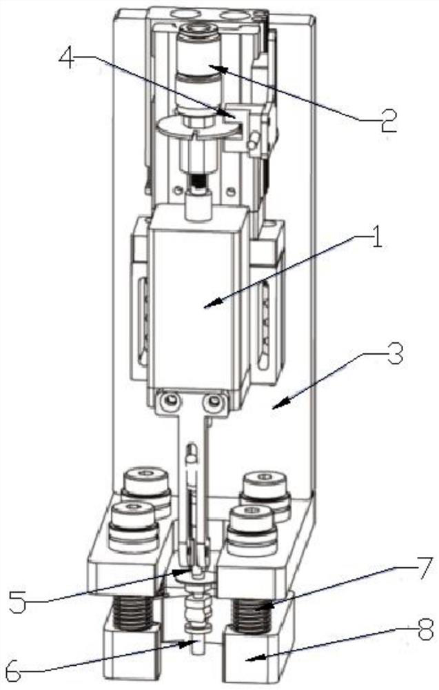
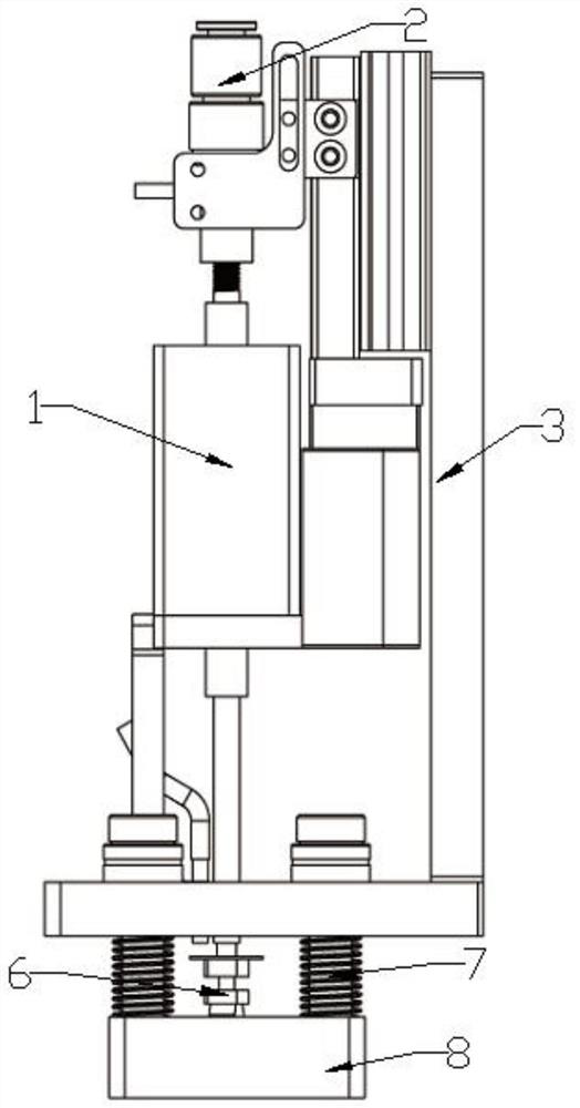
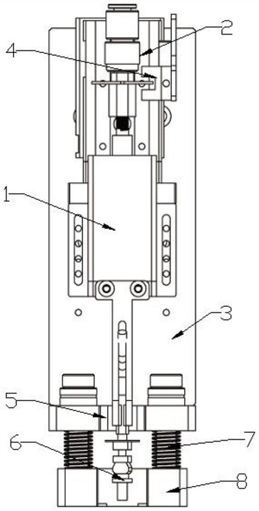
[0021] like Figure 1-4 As shown, a device for detecting chip lamination during testing, including a rotating motor 1, a slide cylinder 2, a main board 3, a rotation sensor 4, a buffer device 6 and a socket pressing block 8, and the slide cylinder 2 is fixed on the main board by bolts 3, the piston end of the sliding table cylinder 2 is connected to the rotating motor 1 through an aluminum block, and is tightened by bolts so that the rotating motor 1 can be driven up and down by the sliding table cylinder 2; the upper cover of the sliding table cylinder 2 is equipped with a rotating The sensor 4 and the buffer device 6 are installed on the output end of the rotary motor 1, and the buffer device 6 is driven to rotate by the rotary motor 1, and the optical fiber sensor 5 is also installed on the aluminum block of the rotary motor 1, and two Socket pressing blocks 8 are symmetrically installed on the main board 3, and insert the pressing spring 7 thereon.

[0022] Induction shee...

Embodiment 2

[0025] like Figure 1-4 As shown, the main board 3 is an L-shaped plate composed of an aluminum fixing plate and an aluminum base plate, the slide cylinder 2 is fixed on the aluminum fixing plate, and the Socket pressing block 8 is fixed on the aluminum base plate.


PUM


Abstract

The invention discloses an apparatus for detecting lamination of chips in a test. The apparatus comprises a rotating motor, a sliding cylinder, a main board, a rotation sensor, a buffer device and Socket pressing blocks, wherein the sliding cylinder is fixed on the main board by bolts, and a piston end of the sliding cylinder is connected with the rotating motor through an aluminum block and is tightened by a bolt. The rotating sensor is mounted on an upper cover portion of the sliding cylinder. The buffer device is mounted on an output end of the rotating motor, and an optical fiber sensor isalso mounted on the aluminum block of the rotating motor. The two Socket pressing blocks are symmetrically mounted on the bottom end of the main board, and pressing springs are nested thereon. The present invention provides an apparatus for detecting lamination of chips in a test, is suitable for chip automatic test equipment, is capable of accurately determining whether the chips are laminated in the Socket or whether foreign matter exists. Installing the apparatus for detecting the lamination of chips can greatly improve the discovery and processing efficiency of the production abnormality,and further improve the intelligent process of the factory.

Description

technical field [0001] The invention relates to the technical field of spectacle lens products, in particular to a device for inspecting chip laminations during testing. Background technique [0002] Integrated circuits or microcircuits, microchips, and chips are a way of miniaturizing circuits (mainly including semiconductor devices, including passive components, etc.) in electronics. They are usually manufactured on the surface of semiconductor wafers, and the circuits are manufactured on The integrated circuit on the surface of the semiconductor chip is also called thin film integrated circuit; another kind of thick film hybrid integrated circuit is a miniaturized circuit composed of independent semiconductor equipment and passive components integrated into the substrate or circuit board; the production process of the chip requires The testing equipment detects the chip to ensure the quality of the chip. [0003] The current test equipment does not have a detection devic...

Claims


Application Information

Patent Timeline
Patent Type & Authority Patents(China)
IPC IPC(8): H01L21/66
CPCH01L22/30
Inventor 邓旭军姜胜林赵俊方盼张少军
Owner SHENZHEN KINGCOS AUTOMATION ROBOT EQUIP CO LTD
Why Eureka
Try Eureka