Method for transferring micro LEDs and display panel

A technology of micro light-emitting diodes and transfer methods, which is applied in the manufacturing of electrical components, electric solid-state devices, semiconductor/solid-state devices, etc. The effect of shortening transfer time and improving production efficiency

Active Publication Date: 2019-04-05
TIANMA MICRO ELECTRONICS CO LTD
View PDF4 Cites 29 Cited by
  • Summary
  • Abstract
  • Description
  • Claims
  • Application Information

AI Technical Summary

Problems solved by technology

[0004] The existing mass transfer technology relies on the transfer head for chip transfer, which requires high transfer accuracy. The transfer head needs to accurately pick up the Micro-LED chip and place it on the target point of the display master, which affects the accuracy of the device. Very demanding and prone to defects
And the transfer efficiency is low, such as assembling a resolution of 4K (K=2 10 ) display device, a single transfer head needs to pick up and place 25KK Micro-LED chips on the receptor substrate, the traditional transfer equipment can only transfer about 25K chips per hour, and it takes more than a month to assemble a device at such a speed Time, in order to solve this problem, some units proposed to use a transfer device with multiple transfer heads, but the precision requirements are very high, the yield rate is low, and technical problems are difficult to break through, which is not conducive to the commercial mass production of products, and the marketization of Micro-LED technology. difficulty

Method used


Image

  • Method for transferring micro LEDs and display panel
  • Method for transferring micro LEDs and display panel
  • Method for transferring micro LEDs and display panel

Examples


Embodiment Construction

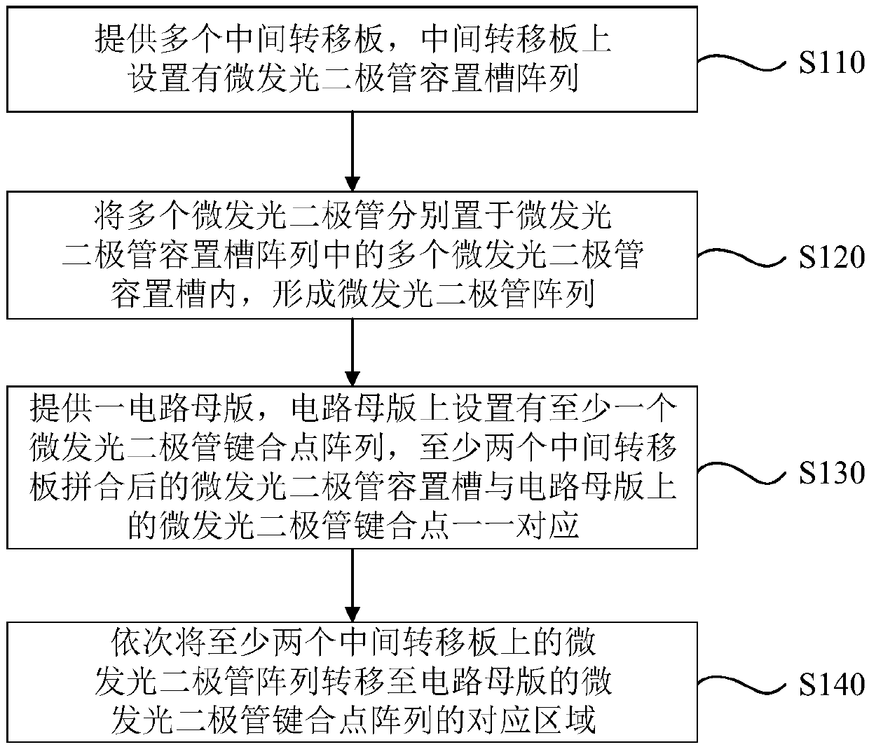
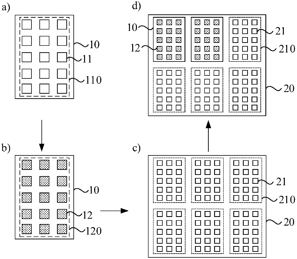
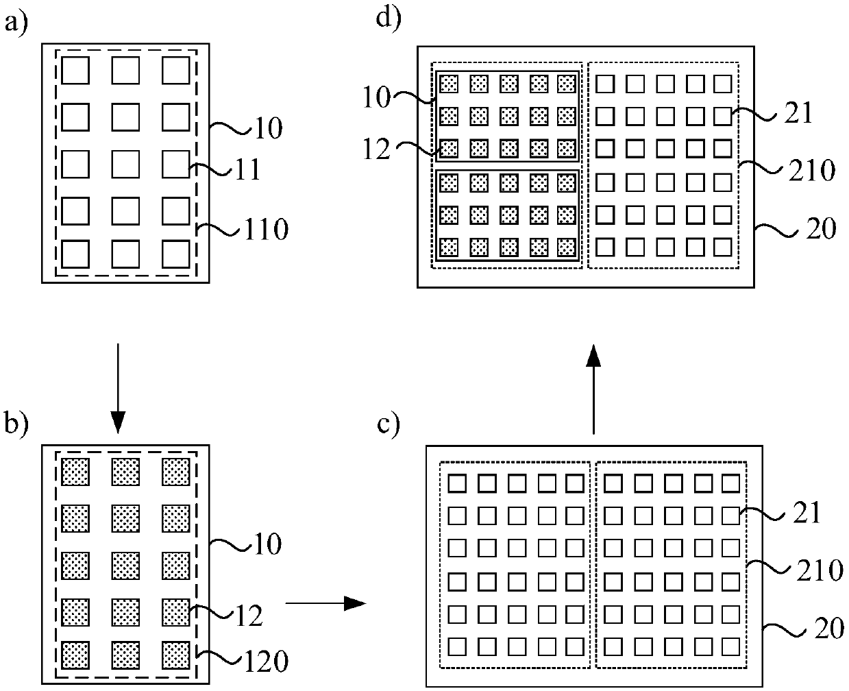
[0053] The present invention will be further described in detail below in conjunction with the accompanying drawings and embodiments. It should be understood that the specific embodiments described here are only used to explain the present invention, but not to limit the present invention. In addition, it should be noted that, for the convenience of description, only some structures related to the present invention are shown in the drawings but not all structures.

[0054] figure 1 It is a flow chart of a method for transferring micro-light emitting diodes provided by an embodiment of the present invention, figure 2 yes figure 1 The structural flow diagram of the transfer method of the shown micro-light-emitting diode, refer to figure 1 and figure 2 , the transfer method of the micro light emitting diode comprises:

[0055] S110, providing a plurality of intermediate transfer plates 10, the intermediate transfer plate 10 is provided with an array of micro light emitting...


PUM


Abstract

The embodiment of the invention discloses a method for transferring micro LEDs and a display panel. The transfer method includes providing a plurality of intermediate transfer plates provided with micro LED receiving groove arrays; arranging a plurality of micro LEDs in a plurality of micro LED receiving grooves in the micro LED receiving groove arrays to form a micro LED array; providing a circuit motherboard provided with at least one micro LED bonding point array, wherein the micro LED receiving grooves of at least two spliced intermediate transfer plates correspond to the micro LED bondingpoints on the circuit motherboard one to one; successively transferring the micro LED arrays on the at least two intermediate transfer plates to a corresponding region of the micro LED bonding pointarray of the circuit motherboard. The method successively transfers the micro LEDs in batches, and shortens the transfer time and improves the transfer efficiency of the micro LEDs that a method of successively transferring single or a small number of micro LEDs.

Description

technical field [0001] Embodiments of the present invention relate to display technologies, and in particular to a method for transferring micro light emitting diodes and a display panel. Background technique [0002] Micro-LED (Micro Light Emitting Diode, Micro-LED) has become the next-generation liquid crystal display (Liquid Crystal Display, LCD) / organic light-emitting display due to its advantages such as high resolution, high brightness, ultra-power saving, fast response speed and long life. (Organic Light-Emitting Diode, OLED), one of the most dynamic display technologies, has also become a research hotspot for various companies. [0003] In the manufacturing process of Micro-LED display panels, the focus is on the mass transfer technology of Micro-LED chips, that is, the technology of transferring Micro-LED chips on the original substrate for making Micro-LED chips to the circuit master of the display panel. The existing mass transfer technology of semiconductor de...

Claims


Application Information

Patent Timeline
Patent Type & Authority Applications(China)
IPC IPC(8): H01L21/67H01L27/15H01L33/48
CPCH01L21/67144H01L27/156H01L33/486H01L2933/0033
Inventor 韩甲伟秦锋刘金娥李小和王臣
Owner TIANMA MICRO ELECTRONICS CO LTD
Why Eureka
Try Eureka