Wiring method for reinforcing protection on important region of metal protection layer at top layer of chip

A top-layer metal and important area technology, applied in the field of chip technology, can solve problems such as simple connection relationship, failure of the protective layer, single step-down form, etc., and achieve the effect of increasing the safety factor, increasing the difficulty, and improving the protection level

Inactive Publication Date: 2019-04-05
TIANJIN UNIV
View PDF3 Cites 5 Cited by
  • Summary
  • Abstract
  • Description
  • Claims
  • Application Information

AI Technical Summary

Problems solved by technology

However, due to the existing top-layer wiring metal, the form of walking is single, mostly parallel wiring, serpentine wiring, spiral wiring and other topological structures, the connection relationship is simple, and it is easy to be photographed and analyzed by the layout or reverse engineering, making the protective layer invalid.

Method used


Image

  • Wiring method for reinforcing protection on important region of metal protection layer at top layer of chip
  • Wiring method for reinforcing protection on important region of metal protection layer at top layer of chip
  • Wiring method for reinforcing protection on important region of metal protection layer at top layer of chip

Examples


Embodiment Construction

[0020] The present invention has carried out focused evolution and modification for the traditional configuration method of the top metal layer wiring, and can focus on the protection of modules that are easy to leak data on the chip, such as memory modules and data buses.

[0021] 1. The wiring configuration method of the top protective layer:

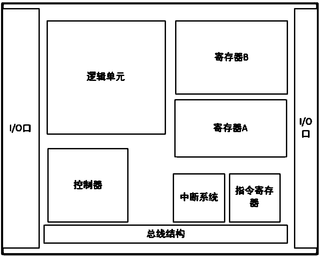
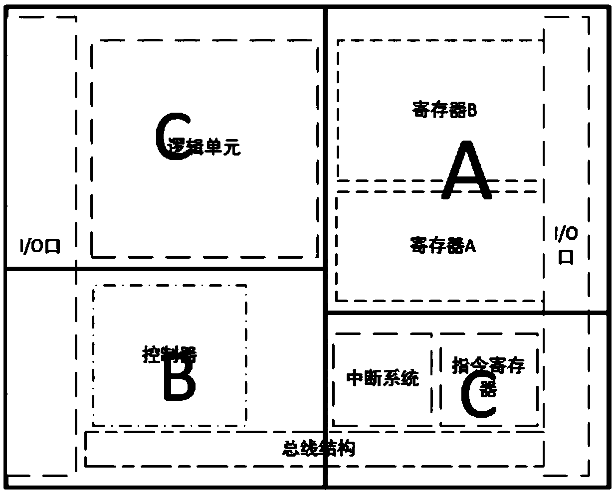
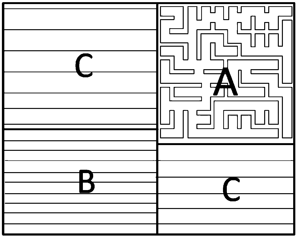
[0022] According to the protection area and degree of protection required by the chip module, the entire wiring layer is divided into multiple wiring areas. figure 1 It is a schematic diagram of the internal layout of a chip. The wiring area is divided into several types according to the security level of the internal structure of the chip, and the number of wiring lines is positively correlated with the security level of the area. Each routing area can be filled with serpentine routing, parallel routing, and random Hamiltonian loops. Among them, the random Hamiltonian circuit image has a high degree of disorder. It can reduce the ...


PUM


Abstract

The invention relates to the field of chip technology and information safety. By the method, the wiring density of a metal wire at a top layer can be improved, the failure area of a shielding line ata key region is reduced, the difficulty on circuit analysis by an attacker is improved, the purpose of important protection on the key region of the chip is achieved, the attacker can be effectively prevented from acquiring internal data of the chip by attack means such as shooting analysis reverse engineering and FIB, and a safety coefficient of the key region of the chip is improved. The wiringmethod for reinforcing protection on the important region of the metal protection layer at the top layer of the chip, disclosed by the technical scheme comprises the steps of firstly, planning wiringregion area and a protection level of each region according to the size of the chip, and dividing a metal shielding layer at the top layer into several wiring regions; and secondly, wiring and fillingeach wiring unit according to a safety coefficient of the wiring region, wherein the wiring number of each region is gradually increased according to the safety level. The method is mainly applied toa chip design and manufacturing occasion.

Description

technical field [0001] The invention relates to the fields of chip technology, information security, etc., and specifically relates to a method for wiring a metal protection layer on the top layer of a chip to strengthen protection for important areas. Background technique [0002] At present, the problem of information security is becoming more and more prominent, and various fields have put forward higher and higher requirements for information security. As the core component of the information system, the integrated circuit chip's security is related to the security of the entire information system. With the continuous advancement of microelectronics technology, physical attack methods against integrated circuit chips are constantly being proposed, and chip security has become an important research proposition in the field of security. [0003] Compared with software security issues, hardware chip security is an undeveloped field. The means of hardware attacking chips a...

Claims


Application Information

Patent Timeline
Patent Type & Authority Applications(China)
IPC IPC(8): H01L23/528H01L23/00G06F17/50
CPCG06F30/392H01L23/528H01L23/573
Inventor 赵毅强甄帅辛睿山蔡里昂赵子龙
Owner TIANJIN UNIV
Why Eureka
Try Eureka