

Superconducting quantum interference device and preparation method
A technology of superconducting quantum interference and devices, which is applied in the direction of magnetic field measurement, instruments, and measuring devices using superconducting devices, can solve problems such as unfavorable SQUID applications, reduce the modulation depth of the magnetic flux-voltage conversion coefficient of SQUID devices, and achieve Large application potential, high sensitivity, low noise effect
- Summary
- Abstract
- Description
- Claims
- Application Information
AI Technical Summary
Problems solved by technology
Method used
Image

Examples
Embodiment 1
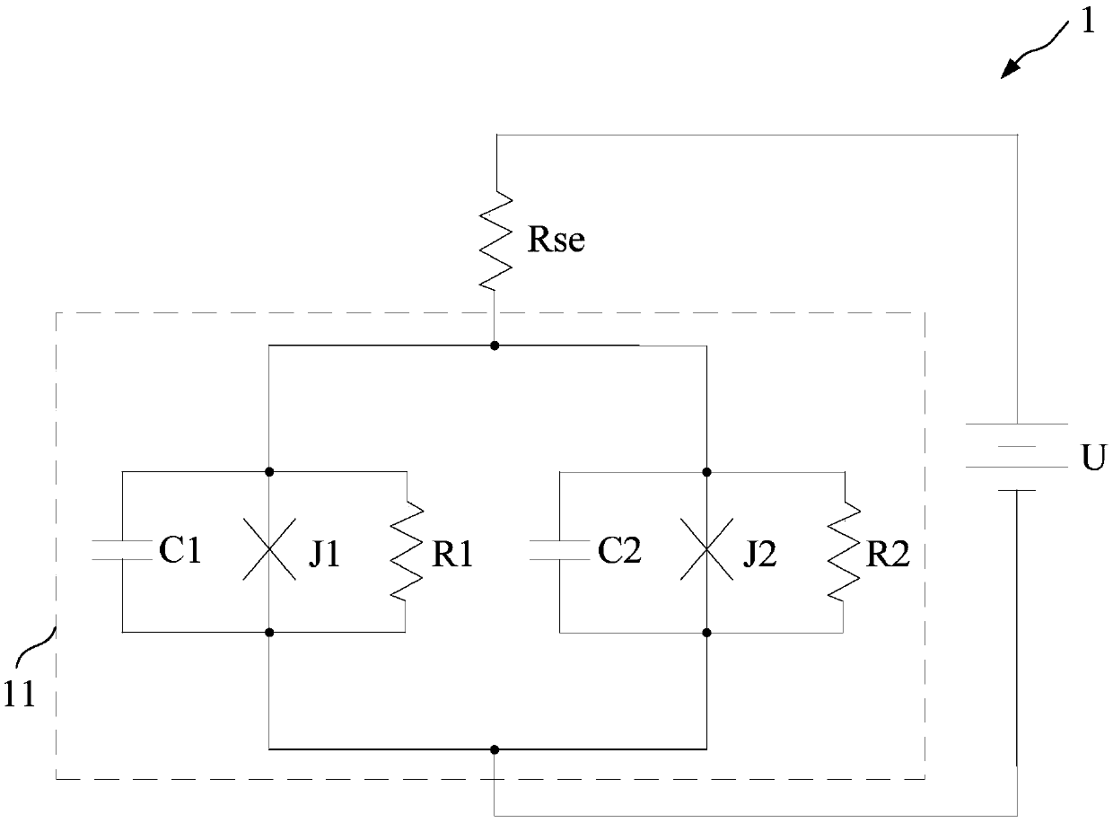
[0035] Such as figure 1 As shown, the present embodiment provides a superconducting quantum interference device 1, and the superconducting quantum interference device 1 includes:
[0036] Underdamped SQUID11 and series resistor Rse.
[0037] Such as figure 1 As shown, the underdamped SQUID11 is connected in series with the series resistor Rse.
[0038] Specifically, the underdamped SQUID11 includes a superconducting ring composed of a first Josephson junction J1 and a second Josephson junction J2 connected in parallel, and a first shunt resistor R1 is connected in parallel to both ends of the first Josephson junction J1 , the two ends of the second Josephson junction J2 are connected in parallel with a second shunt resistor R2. Such as figure 1 As shown, the two ends of the first Josephson junction J1 are also connected in parallel with the equivalent capacitance C1 of the first Josephson junction J1, and the two ends of the second Josephson junction J2 are also connected ...
Embodiment 2
[0051] This embodiment provides the preparation method of the superconducting quantum interference device 1, the preparation method of the superconducting quantum interference device 1 simultaneously prepares the series resistance in the process step of preparing the shunt resistance, and the specific steps are as follows:
[0052] 1) Provide a substrate, sequentially deposit a first superconducting material layer, a first insulating material layer and a second superconducting material layer on the substrate, etch the first superconducting material layer, the first The insulating material layer and the second superconducting material layer form a superconducting loop and a bottom electrode structure.
PUM
| Property | Measurement | Unit |
|---|---|---|
| Resistance | aaaaa | aaaaa |
Abstract
Description
Claims
Application Information