Full-screen display panel and manufacturing method thereof

A technology of full-screen display and production method, which is applied in semiconductor/solid-state device manufacturing, organic semiconductor devices, electrical components, etc., and can solve problems affecting Panel reliability, Panel loss of functionality, crack extension, etc.

Inactive Publication Date: 2019-04-12
WUHAN CHINA STAR OPTOELECTRONICS SEMICON DISPLAY TECH CO LTD
View PDF6 Cites 54 Cited by
  • Summary
  • Abstract
  • Description
  • Claims
  • Application Information

AI Technical Summary

Problems solved by technology

For the O-Cut area, although devices and wiring in the Array section can be avoided, in the OLED manufacturing process, the hole injection layer, hole transport layer, light emitting layer, electron transport layer, electron injection layer, cathode layer, etc. It is generated by evaporation of an open mask (OpenMask). After cutting the O-Cut area, the organic layer of the OLED will be exposed on the cut surface. Due to the physical properties of the inorganic film layers in the TFT array layer and thin film packaging layer, these inorganic film layers are prone to cracks (crack) and crack extension during the O-Cutting process, which will subsequently affect the reliability of the Panel

Method used


Image

  • Full-screen display panel and manufacturing method thereof
  • Full-screen display panel and manufacturing method thereof
  • Full-screen display panel and manufacturing method thereof

Examples


Embodiment Construction

[0049] In order to further illustrate the technical means adopted by the present invention and its effects, the following describes in detail in conjunction with preferred embodiments of the present invention and accompanying drawings.

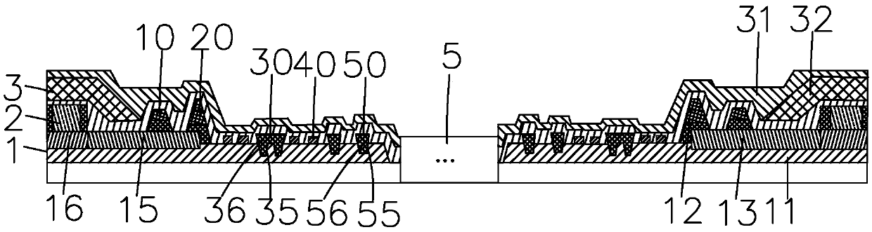
[0050] see Figure 1-2 The present invention firstly provides a full-screen display panel, including an array substrate 1 , an OLED functional layer 2 disposed on the array substrate 1 , and a thin film encapsulation layer 3 covering the OLED functional layer 2 on the array substrate 1 .

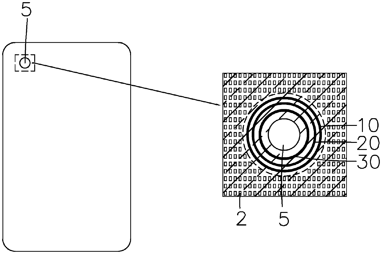
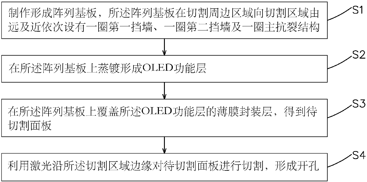
[0051]Specifically, the full-screen display panel of the present invention adopts an O-Cut design, which is provided with an O-shaped opening 5 formed by cutting through its upper and lower surfaces for subsequent placement of a camera or other components.

[0052] Specifically, the array substrate 1 includes a multi-layer inorganic insulating layer 11, a multi-layer organic layer 12 disposed on the multi-layer inorganic insulating layer 11, a multi-layer me...


PUM


Abstract

The invention provides a full-screen display panel and a manufacturing method thereof. The full-screen display panel provided by the invention comprises an array substrate, an OLED functional layer and a thin film packaging layer, wherein an opening hole which is formed by cutting and runs through the upper and lower surfaces of the full-screen display panel is formed in the full-screen display panel; the array substrate is provided with a circle of first retaining wall, a circle of second retaining wall and a circle of main anti-cracking structure from the periphery of the opening hole to theopening hole from far to near in sequence; and the main anti-cracking structure comprises a hollow-out anti-cracking channel formed in a multilayer inorganic insulating layer, and an organic anti-cracking strip which is used for correspondingly filling the anti-cracking channel. Structure optimization is carried out on the cutting peripheral area of the opening hole, so that the crack extension of an inorganic film layer in the array substrate and the thin film packaging layer caused by the cutting process of the opening hole can be prevented.

Description

technical field [0001] The invention relates to the field of display technology, in particular to a flexible full-screen display panel and a manufacturing method thereof. Background technique [0002] In flat panel display technology, Organic Light-Emitting Diode (OLED) displays have the advantages of thinness, active light emission, fast response speed, large viewing angle, wide color gamut, high brightness, low power consumption, and flexible screens can be prepared, etc. Many excellent characteristics have aroused great interest in the scientific research community and the industry, and gradually become the third-generation display technology after Liquid crystal displays (LCD). [0003] Nowadays, the design of "full screen" has become the mainstream of the times, and all suppliers are focusing on the research and development of full-screen products with a higher screen-to-body ratio. For example, the notch screen design adopted by the iPhone X mobile phone can reach 81....

Claims


Application Information

Patent Timeline
Patent Type & Authority Applications(China)
IPC IPC(8): H01L27/32H01L51/52
CPCH10K59/00H10K59/12H10K50/84H10K50/844H10K59/122H10K59/124H10K59/131H10K71/00H10K71/16H10K59/1201H10K2102/311
Inventor 李雪孙亮曾勉王硕晟
Owner WUHAN CHINA STAR OPTOELECTRONICS SEMICON DISPLAY TECH CO LTD
Why Eureka
Try Eureka