Hard film layer reparation device of fingerprint sensor

A fingerprint sensor and hard film technology, which is applied in the field of hard film repair devices, can solve the problems of high cost loss, easy adhesion of external oil or dust, and influence on the surface cleanliness and cleanliness of fingerprint identification keys, etc., to achieve The effect of smooth surface, low cost and simple repair process

Inactive Publication Date: 2019-04-16
AENEQ CO LTD
View PDF0 Cites 0 Cited by
  • Summary
  • Abstract
  • Description
  • Claims
  • Application Information

AI Technical Summary

Problems solved by technology

[0002] In electronic devices such as mobile communication devices and tablet computers, in order to enhance the security performance of electronic devices and prevent the leakage of relevant user information, some manufacturers use optics, acoustics, biosensors and biostatistics principles, and according to the inherent physiological characteristics of the human body, , such as the uniqueness of features such as face, iris, and fingerprints, design and develop biometric buttons for electronic devices with human biometric functions. This type of electronic device uses buttons to identify and verify the inherent physiological characteristics of the human body to determine Whether to start the relevant programs of electronic equipment has many advantages such as safety and reliability, and the most commonly used of this type of buttons is the button with fingerprint recognition function, that is, the fingerprint sensor. When the button is in use, its surface is easy to adhere to external oil or Dust, when the human body is used and operated, will also adhere to human finger sweat and fingerprints, seriously affecting the surface cleanliness and cleanliness of the fingerprint identification buttons. Therefore, fingerprint sensors on the market often have a protective film layer on the top layer, but now Some fingerprint sensors often cannot fully guarantee the smooth surface of the film layer, and in the prior art, the above-mentioned film layer cannot be effectively repaired, but the entire fingerprint sensor can only be discarded, and the cost loss is relatively large.

Method used


Image

  • Hard film layer reparation device of fingerprint sensor
  • Hard film layer reparation device of fingerprint sensor
  • Hard film layer reparation device of fingerprint sensor

Examples


Embodiment Construction

[0023] The following are specific embodiments of the present invention and in conjunction with the accompanying drawings, the technical solutions of the present invention are further described, but the present invention is not limited to these embodiments.

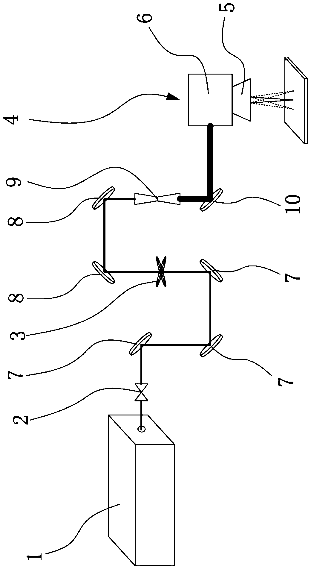
[0024] refer to figure 1 , the present embodiment is a device for repairing the hard film layer of a fingerprint sensor, including a laser emitter 1, an attenuator 2, a polarizer 3, a beam expander 9 and an etcher 4 arranged in sequence, and the polarizer 3 and the attenuator 2 At least one first reflector 7 is arranged between them, at least one second reflector 8 is arranged between the beam expander 9 and the polarizer 3, at least one third reflector is arranged between the etcher 4 and the beam expander 9 10. The first reflector 7, the second reflector 8 and the third reflector 10 are all used to collimate the laser beam.

[0025] Further, the etcher 4 includes a field mirror 5, an etching mirror, a motor, and a scan...


PUM


Abstract

The invention provides a hard film layer reparation device of a fingerprint sensor, and belongs to the technical field of electronic equipment. The problems that the surface of an existing hard film layer of a fingerprint sensor is not level enough, and the hard film layer cannot be repaired and can only by discarded are solved. The hard film layer reparation device of the fingerprint sensor comprises a laser emitter, an attenuator, a polarizer and an etcher which are sequentially arranged. The etcher comprises a field lens used for etching the hard film layer. Scanning type etching is carriedout on an epoxy resin coating on the surface of the fingerprint sensor, the non-level epoxy resin coating is removed, and coating is carried out again; and the reparation process is simple, and consumption is low.

Description

technical field [0001] The invention belongs to the technical field of electronic equipment, and relates to a device for repairing a hard film layer of a fingerprint sensor. Background technique [0002] In electronic devices such as mobile communication devices and tablet computers, in order to enhance the security performance of electronic devices and prevent the leakage of relevant user information, some manufacturers use optics, acoustics, biosensors and biostatistics principles, and according to the inherent physiological characteristics of the human body, , such as the uniqueness of features such as face, iris, and fingerprints, design and develop biometric buttons for electronic devices with human biometric functions. This type of electronic device uses buttons to identify and verify the inherent physiological characteristics of the human body to determine Whether to start the relevant programs of electronic equipment has many advantages such as safety and reliability...

Claims


Application Information

Patent Timeline
IPC IPC(8): B23K26/362B23K26/064B23K26/082
CPCB23K26/362B23K26/064B23K26/0643B23K26/0648B23K26/082
Inventor 赖耀升金渶桓江建志邹嘉瑞
Owner AENEQ CO LTD
Why Eureka
Try Eureka