Display panel

A display panel and pixel technology, applied in nonlinear optics, instruments, optics, etc., can solve the problems of asymmetric viewing angle, reduced transmittance, and difficulty in taking into account excellent viewing angle performance, so as to improve the transmittance and reduce the amount of light transmission. the effect of the loss

Active Publication Date: 2019-04-16
SHENZHEN CHINA STAR OPTOELECTRONICS SEMICON DISPLAY TECH CO LTD
View PDF2 Cites 30 Cited by
  • Summary
  • Abstract
  • Description
  • Claims
  • Application Information

AI Technical Summary

Problems solved by technology

[0004] With the full promotion of large-size displays, HVA (High Vertical Alignment) technology with 8-domain pixel electrode design has been widely used due to its excellent viewing angle performance. The trunk (trunk), so its transmittance is significantly reduced, and although the 4domain pixel electrode design used to improve the transmittance has achieved an increase in transmittance, it is difficult to take into account the excellent viewing angle performance of the original 8domain pixel electrode, thus There are bad problems such as viewing angle asymmetry and color shift.
[0005] like figure 1 As shown, in the existing 8domain pixel electrode design, the deflection direction of the electric field on both sides of the vertical trunk is along the slit of the electrode branch, which leads to confusion of liquid crystal inversion on or around the trunk, greatly reduces the efficiency of the liquid crystal, and causes trunk A large number of dark lines appear in and around the area, which directly leads to the decrease of the penetration rate
In addition, in the existing HG2D pixel architecture, the opaque data line (data line) sacrifices a lot of transmittance

Method used


Image

  • Display panel
  • Display panel
  • Display panel

Examples


Embodiment Construction

[0029] In order to further illustrate the technical means adopted by the present invention and its effects, the following describes in detail in conjunction with preferred embodiments of the present invention and accompanying drawings.

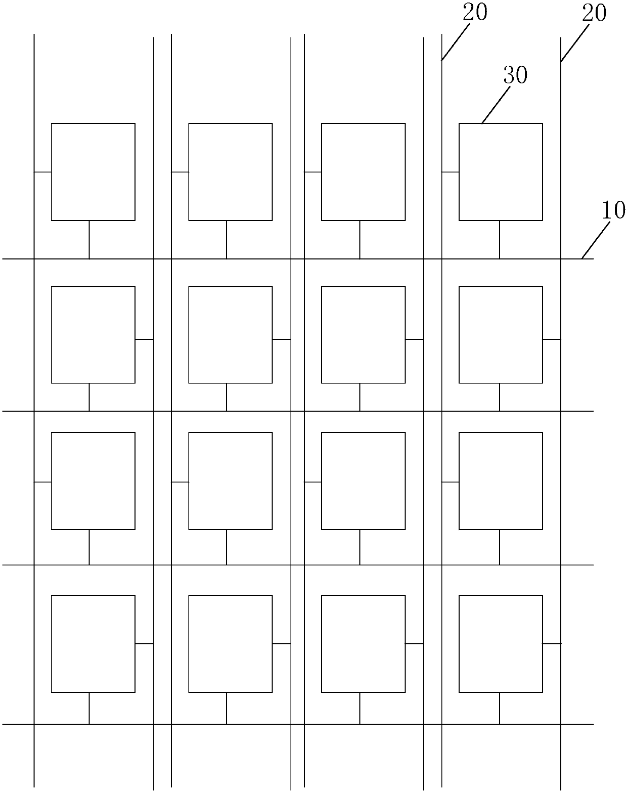
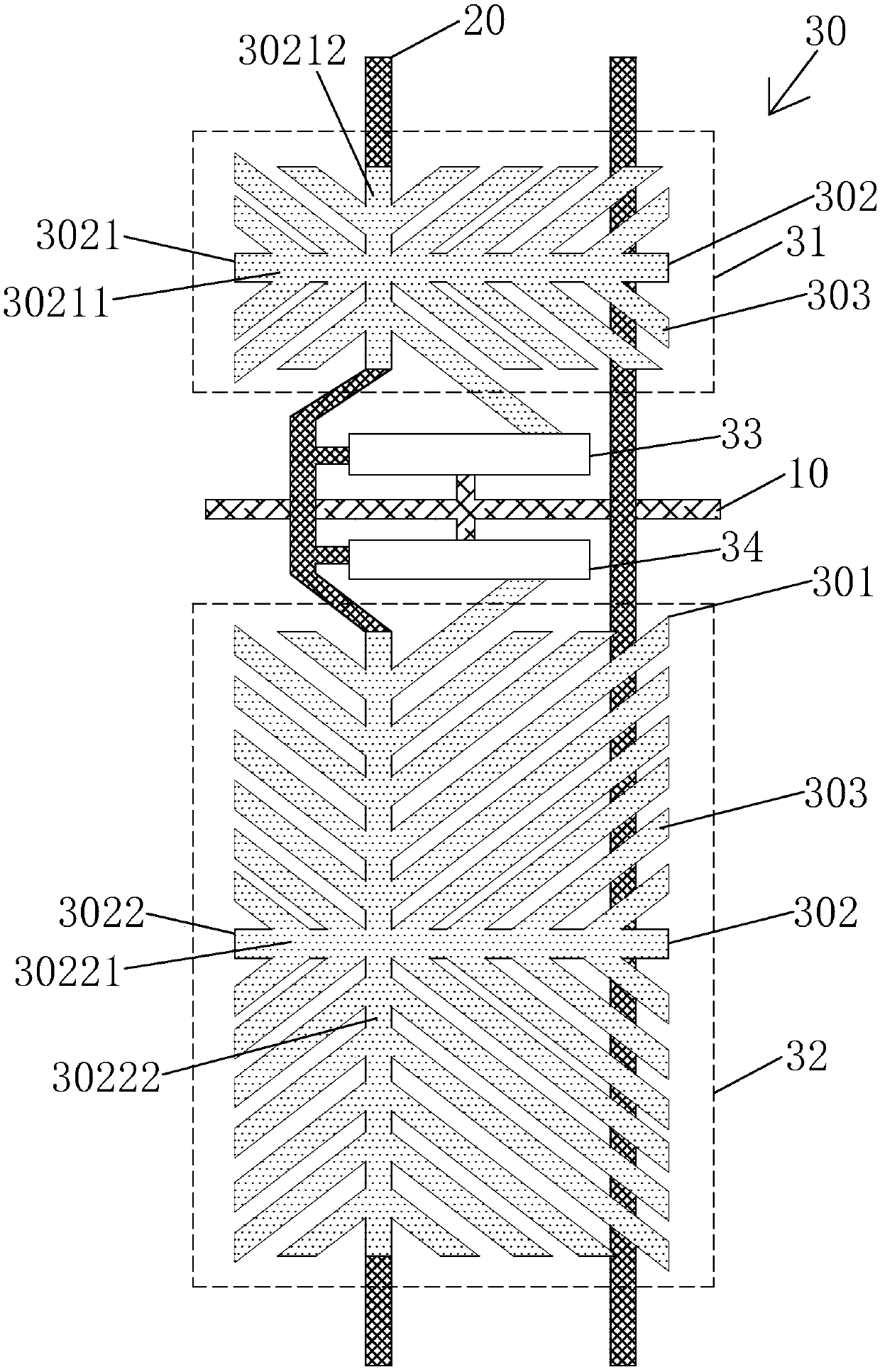
[0030] see Figure 2 to Figure 5 , the present invention provides a display panel, comprising: a plurality of scanning lines 10 extending in the horizontal direction, a plurality of data lines 20 extending in the vertical direction, and a plurality of sub-pixels 30 arranged in an array;

[0031] Each scanning line 10 is connected to a row of sub-pixels 30; every two data lines 20 are respectively connected to odd-numbered rows of sub-pixels 30 and even-numbered rows of sub-pixels 30 in a column of sub-pixels 30;

[0032] The sub-pixel 30 includes a pixel electrode 301; the pixel electrode 301 includes a trunk electrode 302 that divides the sub-pixel 30 into several domains;

[0033] The main electrode 302 of the sub-pixel 30 overlaps with the...


PUM


Abstract

The invention provides a display panel. The display panel comprises a plurality of scanning lines extending along the horizontal direction, a plurality of data lines extending along the vertical direction and a plurality of sub-pixels arranged in an array, wherein each scanning line is connected with a row of sub-pixels, each two data lines are respectively connected with odd-numbered row sub-pixels and even-numbered row sub-pixels in a column of sub-pixels, each sub-pixel includes a pixel electrode, the pixel electrode includes a trunk electrode dividing the sub-pixels into a plurality of domains, and the trunk electrode of the sub-pixel is overlapped with the data line connected with the sub-pixel, so that the light-proof data lines are enabled to cover the trunk electrodes and peripheral dark lines thereof, the loss of the light transmission is greatly reduced, and the penetration rate is effectively improved.

Description

technical field [0001] The present invention relates to the field of display technology, in particular to a display panel. Background technique [0002] Thin Film Transistor (TFT) is the main driving element in current Liquid Crystal Display (LCD) and Active Matrix Organic Light-Emitting Diode (AMOLED). It is related to the display performance of the flat panel display device. [0003] Most of the liquid crystal displays currently on the market are backlight liquid crystal displays, which include a liquid crystal display panel and a backlight module. The working principle of the liquid crystal display panel is to pour liquid crystal molecules between the thin film transistor array substrate (ThinFilm Transistor Array Substrate, TFT Array Substrate) and the color filter (ColorFilter, CF) substrate, and apply pixel voltage on the two substrates respectively. and the common voltage, through the electric field formed between the pixel voltage and the common voltage to control ...

Claims


Application Information

Patent Timeline
Patent Type & Authority Applications(China)
IPC IPC(8): G02F1/1362G02F1/1343
CPCG02F1/134309G02F1/136286
Inventor 张银峰林永伦李轩
Owner SHENZHEN CHINA STAR OPTOELECTRONICS SEMICON DISPLAY TECH CO LTD
Why Eureka
Try Eureka