LDO circuit

A technology of circuits and suppression circuits, which is applied in the direction of adjusting electric variables, control/regulation systems, instruments, etc., to achieve the effect of eliminating overshoot

Active Publication Date: 2019-04-19
SHANGHAI HUAHONG GRACE SEMICON MFG CORP
View PDF4 Cites 8 Cited by
  • Summary
  • Abstract
  • Description
  • Claims
  • Application Information

AI Technical Summary

Problems solved by technology

[0003] figure 1 The disadvantage of the circuit structure shown is that the LDO output voltage V_LDO will overshoot when the power is turned on, and the LDO output voltage V_L

Method used


Image

  • LDO circuit
  • LDO circuit
  • LDO circuit

Examples


Embodiment Construction

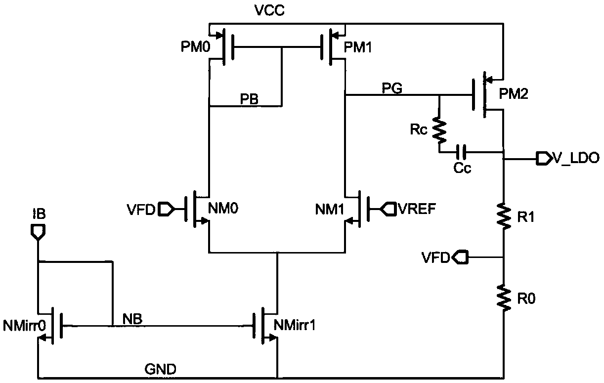
[0032] first review as figure 1 Existing LDO circuit diagram shown; applicant's figure 1 The technical problems existing in the circuit shown are analyzed as follows, figure 1 The circuit shown in the figure only produces LDO output voltage overshoot during power-on, because it takes a certain amount of time for the feedback loop to stabilize, that is, it takes a certain amount of time for the nodes PG and PB to reach a stable value, and the node PG passes through The current flowing out of the PMOS tube PM1 increases the charging of the compensation capacitor Cc. During the power-on process, the current of the PMOS tube PM1 is small, so the charging current of the compensation capacitor Cc is small, so that the node PG rises faster during the power-on process. It should be less than the rising rate of the power supply voltage VCC, so the source-gate voltage of the PMOS transistor PM2 will maintain a large value during the power-on process, so that the PMOS transistor PM2 wil...


PUM


Abstract

The invention discloses an LDO circuit, which comprises an overshoot suppression circuit and an LDO main circuit; the overshoot suppression circuit comprises a current comparator, wherein the currentcomparator comprises two comparison current sources and a second PMOS tube serving as a switch between the two comparison current sources; and the grid electrode of the second PMOS tube is connected with the grid electrode of a mirror image NMOS tube corresponding to the tail current. The overshoot suppression circuit also includes a first capacitor and a third PMOS tube. The drain of the third PMOS tube is connected to the gate of the first PMOS tube of the LDO body circuit. In the electrifying process, before the power supply voltage rises to be less than or equal to the sum of the thresholdvoltages of the mirror NMOS tube and second PMOS tube, the second PMOS tube is turned off, the first comparison current source pulls down the gate voltage of the third PMOS tube so that the gate voltage of the first PMOS tube changes along with the power supply voltage, thereby preventing power-on overshoot; and the third PMOS tube is disconnected after the power-on is finished so as to avoid influencing the LDO main circuit.

Description

technical field [0001] The invention relates to a semiconductor integrated circuit manufacturing, in particular to a low-dropout linear regulator (LDO) circuit. Background technique [0002] Such as figure 1 Shown is the existing LDO circuit diagram; the existing LDO circuit includes a differential amplifier, PMOS transistor PM2 and a resistor string composed of resistors R0 and R1. One input terminal of the differential amplifier is connected to the reference voltage VREF, and the other input terminal is connected to the resistor The series divides the LDO output voltage V_LDO to form the feedback voltage VFD, the drain of the PMOS transistor PM2 outputs the LDO output voltage V_LDO, and the source of the PMOS transistor PM2 is connected to the power supply voltage VCC. figure 1 The differential amplifier shown in includes a differential amplifier main circuit composed of NMOS transistors NM0 and NM1, an active load circuit composed of PMOS transistors PM0 and PM1, and a m...

Claims


Application Information

Patent Timeline
IPC IPC(8): G05F1/56
CPCG05F1/56
Inventor 周宁
Owner SHANGHAI HUAHONG GRACE SEMICON MFG CORP
Why Eureka
Try Eureka