Pixel compensation method, pixel compensation circuit and display

A technology of compensation circuit and compensation method, which is applied in the direction of static indicators, instruments, etc., can solve the problems of drift, pixel charging ability affecting the display effect and change of the liquid crystal panel, and achieve the effect of avoiding afterimage and flicker

Active Publication Date: 2019-04-19
XIANYANG CAIHONG OPTOELECTRONICS TECH CO LTD
View PDF10 Cites 11 Cited by
  • Summary
  • Abstract
  • Description
  • Claims
  • Application Information

AI Technical Summary

Problems solved by technology

For the properties of amorphous silicon TFT itself, as long as there is a voltage difference between the gate and the source/drain for a long time, the I-V characteristics of the TFT will change, that is, the same gate-source voltage V GS Next, the leakage current I D will drift
For the pixels of the liquid crystal panel, u

Method used


Image

  • Pixel compensation method, pixel compensation circuit and display
  • Pixel compensation method, pixel compensation circuit and display
  • Pixel compensation method, pixel compensation circuit and display

Examples


Embodiment 1

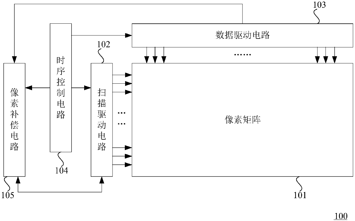
[0048] See image 3 and Figure 4 , image 3 It is a schematic diagram of a circuit structure of a display provided by an embodiment of the present invention, Figure 4 It is a schematic flowchart of a pixel compensation method provided by an embodiment of the present invention. The pixel compensation method is applicable to TFT-LCD displays, and its working principle is also applicable to other displays such as LED displays and OLED displays. The method can effectively solve the problem of insufficient charging of the pixel due to I-V characteristic drift caused by the long-term bias of the TFT during the working process.

[0049] Specifically, the display 100 may include: a pixel matrix 101 , a scan driving circuit 102 , a data driving circuit 103 , a timing control circuit 104 and a pixel compensation circuit 105 . Among them, the pixel compensation circuit 105 is electrically connected to the scan driving circuit 102, the data driving circuit 103 and the timing control...

Embodiment 2

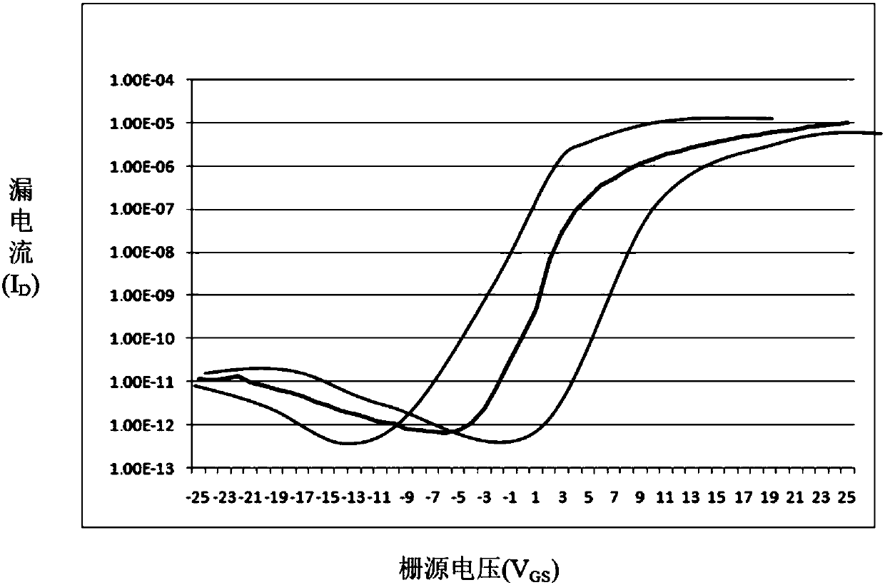
[0057] See Figure 5 and Image 6 , Figure 5 A schematic structural diagram of a pixel compensation circuit provided by an embodiment of the present invention, Image 6 A schematic diagram of an I-V characteristic curve of a TFT provided by an embodiment of the present invention. In this embodiment, on the basis of the foregoing embodiments, the working principle of the pixel compensation circuit and the corresponding pixel compensation method are described in detail as follows.

[0058] The pixel compensation circuit 105 includes a processor 1051 , a memory 1052 and a digital-to-analog converter 1053 . Wherein, the processor 1051 is electrically connected to the memory 1052 and the digital-to-analog converter 1053 respectively.

[0059] Specifically, the memory 1052 stores a look-up table (Look-Up-Table, LUT for short) of compensation voltage values. The LUT is a set of data obtained by testing the I-V characteristics of the TFT under different conditions in advance. Thr...

Embodiment 3

[0071] See Figure 7 and Figure 8 , Figure 7 A logical schematic diagram of a pixel supplementary circuit provided by an embodiment of the present invention, Figure 8 A schematic diagram of a LUT curve provided by an embodiment of the present invention. In this embodiment, on the basis of the above-mentioned embodiments, the principle of the pixel supplement method of the present invention is described in detail by taking a TFT in the AA area and increasing or decreasing the same LUT value at the same time for the turn-on voltage and turn-off voltage of the TFT as an example. .

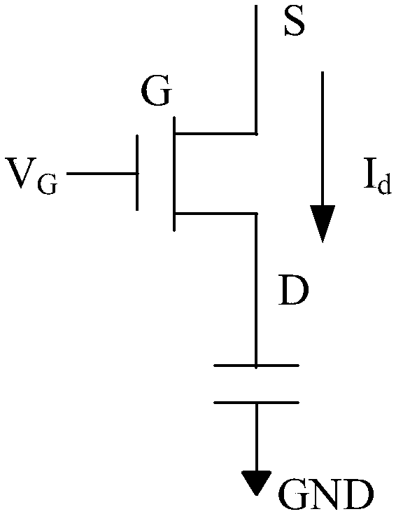
[0072] After starting up, the processing module starts to work, starts to obtain the start-up time point from the timer of the timing control circuit, and starts to obtain the voltage V applied to the TFT gate from the scanning driving circuit and the data driving circuit. G and source voltage V S , while depending on the source voltage V S Calculate the drain voltage V D Or get the drain vo...


PUM


Abstract

The invention relates to a pixel compensation method, a pixel compensation circuit and a display. The pixel compensation method comprises the following steps: recording working hours of the display, and computing grid voltage and source voltage of a TFT at a display region in the working hours, searching the corresponding voltage compensation value from a comparison table according to the workinghours, the grid voltage and the source voltage; and performing voltage compensation on a scanning signal of the display according to the voltage compensation value. Through the pixel compensation method disclosed by the embodiment of the invention, the grid voltage and the source voltage in a time quantum of the display are counted, and the prestored mapping table is searched according to the duration of the time quantum, the statistical values of the grid voltage, the source voltage and the drain voltage so as to determine a voltage adjusting value; the voltage value of a scanning driving signal is adjusted according to the voltage adjusting value, thereby solving the display image ghost or flickering problem caused by the I-V character curve drifting of the TFT due to long-term voltage difference.

Description

technical field [0001] The invention belongs to the technical field of liquid crystal display, and in particular relates to a pixel compensation method, a pixel compensation circuit and a display. Background technique [0002] Thin Film Transistor Liquid Crystal Display (TFT-LCD for short) is a kind of active matrix liquid crystal display (ActI-Ve Matrix Liquid Crystal Display, AM-LCD for short). In terms of comprehensive performance such as power consumption, life span, volume and weight, etc., the display comprehensively exceeds that of a cathode ray tube (Cathode Ray Tube, referred to as CRT). broad. [0003] See figure 1 and figure 2 , figure 1 A schematic structural diagram of a display area TFT provided for the prior art; figure 2 A schematic diagram of an I-V characteristic curve of a selected TFT in a display area provided in the prior art. For the properties of the amorphous silicon TFT itself, as long as there is a voltage difference between the gate and th...

Claims


Application Information

Patent Timeline
IPC IPC(8): G09G3/36
CPCG09G3/3677G09G3/3648G09G2320/0247G09G2320/0257G09G2320/0285G09G3/3688G09G3/3696G09G2310/0251G09G2310/08G09G2320/0219
Inventor 吴永良
Owner XIANYANG CAIHONG OPTOELECTRONICS TECH CO LTD
Why Eureka
Try Eureka