Multiple-bit comparator with reliable output timing and reduced hazards

A bit comparator and comparator technology, applied in the field of comparing multi-bit input signals, can solve problems such as timing design difficulties

Inactive Publication Date: 2002-12-18
LAPIS SEMICON CO LTD
View PDF0 Cites 0 Cited by
  • Summary
  • Abstract
  • Description
  • Claims
  • Application Information

AI Technical Summary

Problems solved by technology

This hazard also creates timing design difficulties, as it must ensure that the output signal is sampled at a point where failure is avoided as much as possible

Method used


Image

  • Multiple-bit comparator with reliable output timing and reduced hazards
  • Multiple-bit comparator with reliable output timing and reduced hazards
  • Multiple-bit comparator with reliable output timing and reduced hazards

Examples


Embodiment Construction

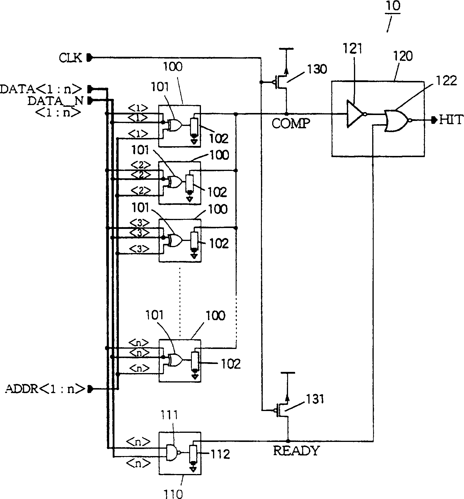
[0047] Embodiments of the present invention are described below with reference to the drawings. Although the embodiments are not limited to a particular manner of use, the embodiments will be described herein in connection with a cache memory in a semiconductor integrated circuit.

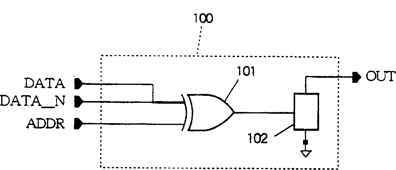
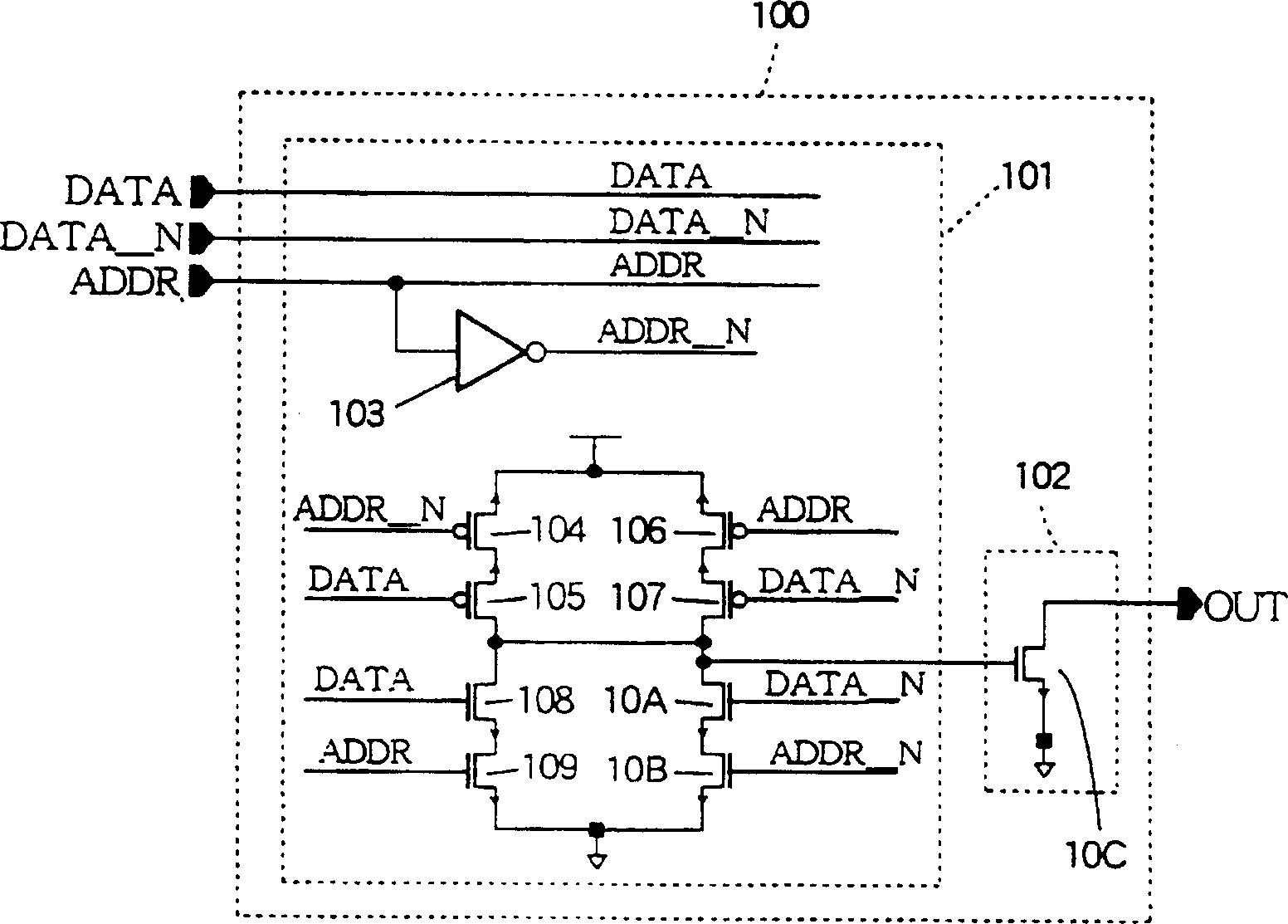
[0048] In the figure, the input signal to be compared is represented by ADDR and DATA. The notation indicates that each signal includes n bits input in parallel, and n is any integer greater than 1. Individual bits are marked to to identify. DATA is received in complementary form, and the complementary input is represented by DATA_N.

[0049] The input signals DATA, DATA_N, and ADDR are synchronized with a clock signal represented by CLK. The clock signal varies between a high level equal to the positive supply potential and a low level equal to zero potential or ground potential. These high and low levels are also the logic levels of the input signals DATA, DATA_N and ADDR. The power pot...


PUM


Abstract

A multi-bit comparator that compares individual bits of a first multi-bit signal with corresponding bits of a second multi-bit signal. The output control circuit in the multi-bit comparator detects whether the second signal is active or inactive based on the change in the second signal, and maintains the output signal at a fixed logic level when the second signal is inactive. When the second signal is active, the output signal is controlled according to the combined result of the respective bit comparisons. The individual bit comparison results are preferably combined using wired OR logic.

Description

field of invention [0001] The present invention relates to a method of comparing multi-bit input signals and multi-bit comparators for use in content addressable memories such as cache memories. technical background [0002] A multi-bit comparator accepts a pair of multi-bit input signals and produces an output signal that indicates whether each bit of the two input signals is the same. In a cache memory, one input signal gives the address of the requested data word, and another input signal gives the address of the superspeed data word. The output signal indicates that if the two addresses are the same, the result is called a cache hit, or if the output signal is different, the result is called a cache miss. [0003] The classic circuit structure of a multi-bit comparator that will be described below consists of an XOR gate that compares the bits of the two output signals, and a NOR gate that combines the outputs of the XOR gates to produce the final output signal. This s...

Claims


Application Information

Patent Timeline
IPC IPC(8): G06F7/04G06F7/02
CPCG06F7/02G06F2207/025
Inventor 黑津悟
Owner LAPIS SEMICON CO LTD
Why Eureka
Try Eureka