Optical part defect detecting device and method

A technology for optical parts and detection devices, applied in the field of image processing, can solve the problems of low detection accuracy of defects and neglect of details of defects, and achieve the effect of improving reliability and improving detection accuracy.

Inactive Publication Date: 2019-04-23
NANJING UNIV OF SCI & TECH
View PDF9 Cites 12 Cited by
  • Summary
  • Abstract
  • Description
  • Claims
  • Application Information

AI Technical Summary

Problems solved by technology

However, in the above methods, the lighting system uses a single-spectrum light source, and the optical parts to be tested are all fixed, resulting in many defect details being ignored, and the defect detection accuracy is not high

Method used


Image

  • Optical part defect detecting device and method
  • Optical part defect detecting device and method
  • Optical part defect detecting device and method

Examples


Embodiment Construction

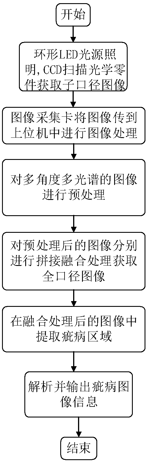
[0020] The solutions of the present invention will be further described below in conjunction with the accompanying drawings and specific embodiments.

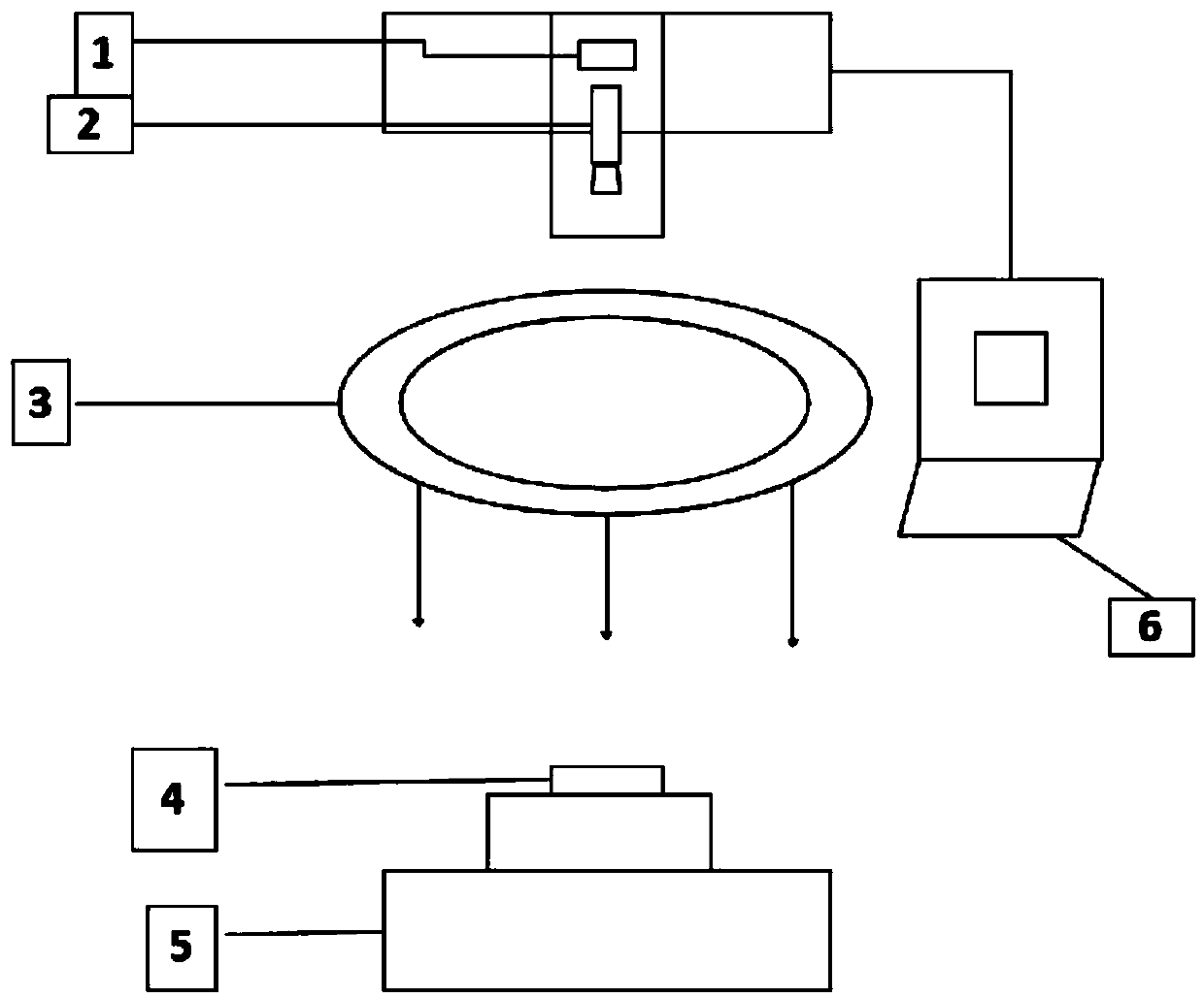
[0021] Such as figure 1 As shown, the optical part surface defect detection device includes an image acquisition module, an illumination system, a motion control module and a processor, and the motion control module is used to place the measured optical part 4 and control the movement of the optical part in the azimuth and pitch directions , the illumination system is used to provide light sources of different spectra for the measured optical parts; the image acquisition module is used to collect images of optical parts with different spectra and different position angles; the processor is used to control the movement of the motion control module, Receive images of optical parts for defect detection.

[0022] In some embodiments, the image acquisition module includes a CCD 1 and a microscope lens 2, and is arranged above the m...


PUM


Abstract

The invention discloses an optical part defect detecting device and method. The device comprises an image collecting module, an illuminating system, a motion control module and a processor; the motioncontrol module is used for placing a to-be-detected optical part and controlling the optical part to move in the orientation and pitching direction. The illuminating system is used for providing light sources with different spectrum for the to-be-detected optical part. The image collecting module is used for collecting the images of the optical part with different spectrum and under different positions and angles. The processor is used for controlling movement of the motion control module and receiving the images of the optical part to conduct defect detection. According to the invention, themulti-spectrum and multi-angle images are obtained through a multi-spectrum LED light source and by rotating the to-be-detected optical part, the multi-spectrum and multi-angle defect image information under the same scene is integrated by the image fusion technology, and the information reliability and detection precision are improved.

Description

technical field [0001] The invention relates to image processing technology, in particular to an optical component defect detection device and method. Background technique [0002] The surface defect is an important evaluation index of the surface quality of optical parts, which will cause scattering and energy loss to the light beam incident on the surface of the optical part. If the size of the defect is small, more serious diffraction phenomenon will occur, and the film Phenomena such as damage, diffraction fringes, energy absorption, and defect distortion further affect the use efficiency and service life of optical components. [0003] The dark-field imaging method based on white light illumination and traditional optical microscopy imaging is currently the mainstream surface defect detection method. In order to improve the detection accuracy, some detection methods improve the imaging system to obtain clear images. For example, patent CN108152299A discloses a high-pr...

Claims


Application Information

Patent Timeline
Patent Type & Authority Applications(China)
IPC IPC(8): G01N21/95G01N21/958G06T7/00G06T5/50
CPCG01N21/8851G01N21/95G01N21/958G01N2021/8887G06T5/50G06T7/0002
Inventor 王志华唐姣姣仝若男高峰
Owner NANJING UNIV OF SCI & TECH
Why Eureka
Try Eureka