A data communication method and system of Arduino Due and an FPGA

A data communication system and data communication technology, applied in the field of communication control, can solve problems such as inability to perform fast data communication, and achieve the effect of fast data interaction

Inactive Publication Date: 2019-04-23
CHANGCHUN INST OF OPTICS FINE MECHANICS & PHYSICS CHINESE ACAD OF SCI
View PDF4 Cites 1 Cited by
  • Summary
  • Abstract
  • Description
  • Claims
  • Application Information

AI Technical Summary

Problems solved by technology

[0004] In view of this, the embodiment of the present application provides a data communication method and system between Arduino Due and FPGA to solve the problem that fast data communication cannot be performed between Arduino Due and FPGA in the prior art

Method used


Image

  • A data communication method and system of Arduino Due and an FPGA
  • A data communication method and system of Arduino Due and an FPGA
  • A data communication method and system of Arduino Due and an FPGA

Examples


Embodiment 1

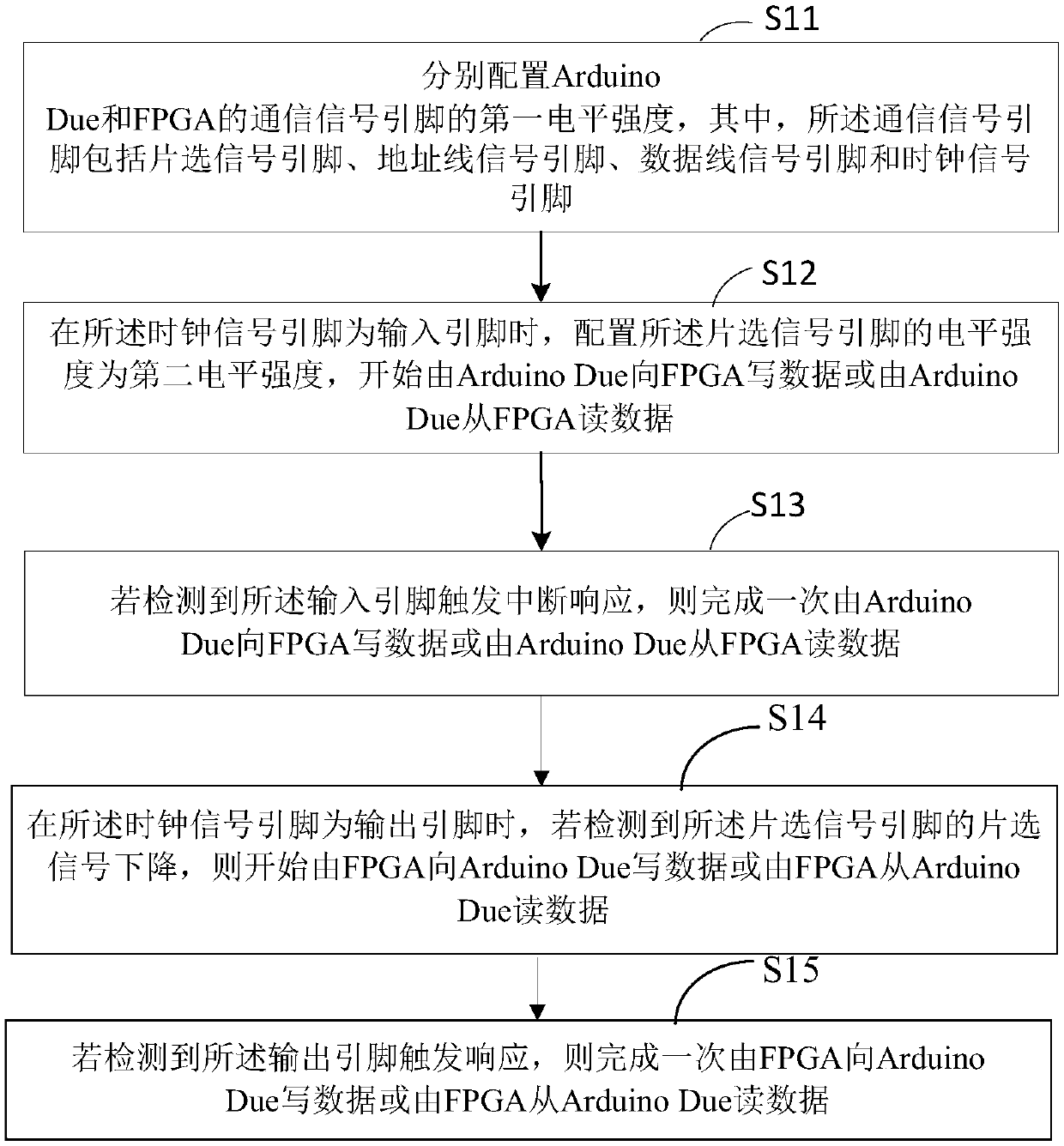
[0047] figure 1 It shows a schematic diagram of a data communication method between Arduino Due and FPGA provided by the embodiment of the present application, including step S11-step S15, wherein:

[0048] Step S21, configure the first level strength of the communication signal pins of Arduino Due and FPGA respectively, wherein the communication signal pins include chip select signal pins, address line signal pins, data line signal pins and clock signals pin;

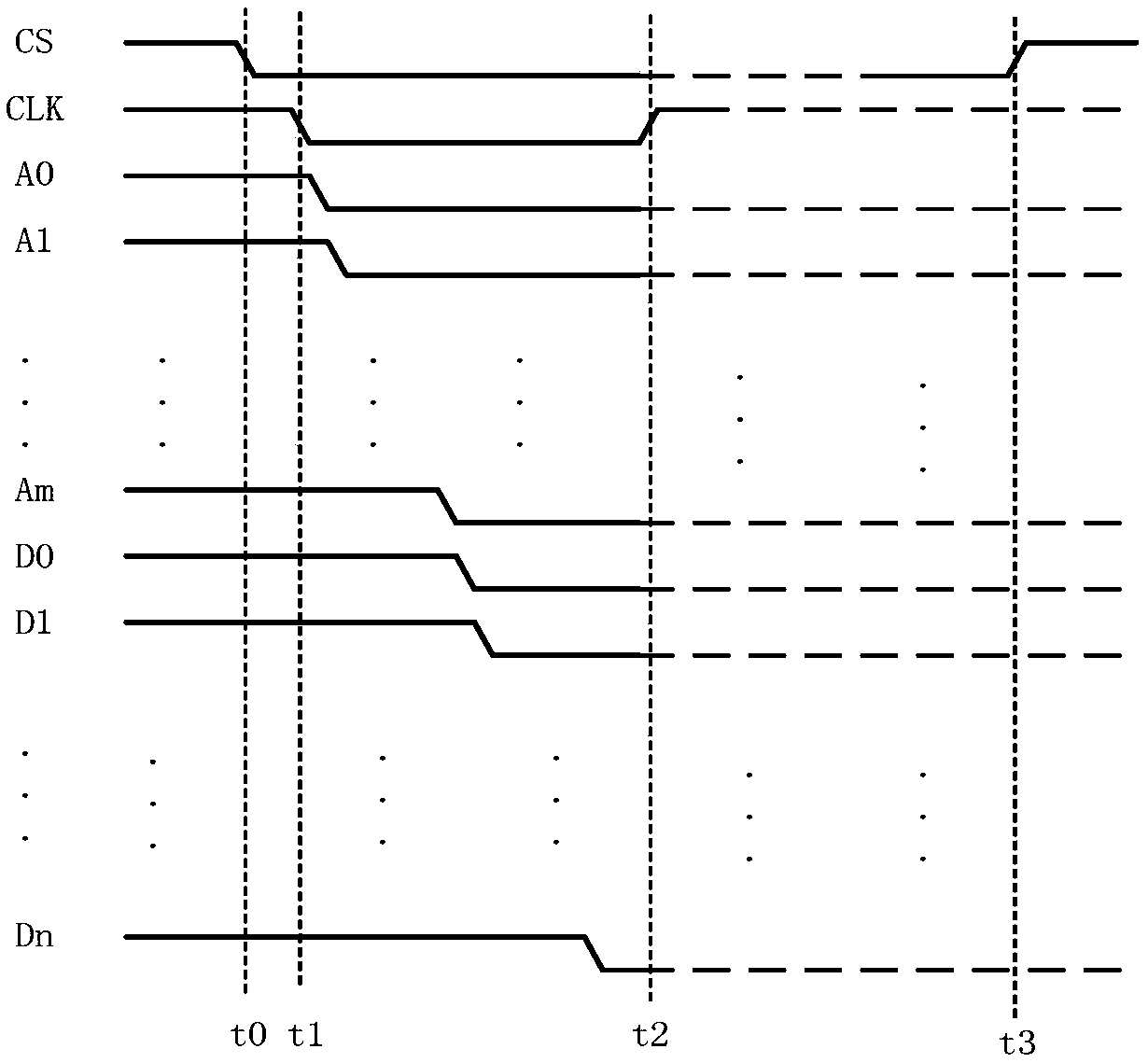
[0049] Step S22, when the clock signal pin is an input pin, configure the level strength of the chip select signal pin to be the second level strength, start to write data to FPGA by Arduino Due or read data from FPGA by Arduino Due data;

[0050] Step S23, if it is detected that the input pin triggers an interrupt response, write data to FPGA by ArduinoDue or read data from FPGA by ArduinoDue;

[0051] Optionally, if it is detected that the input pin triggers an interrupt response, the Arduino Due writes data to th...

Embodiment 2

[0075] Figure 7 It shows a data communication system between Arduino Due and FPGA provided by another embodiment of the present application, and the data communication system includes:

[0076] Configuration module 71, is used to configure the first level intensity of the communication signal pin of Arduino Due and FPGA respectively, wherein, described communication signal pin comprises chip selection signal pin, address line signal pin, data line signal pin and clock signal pins;

[0077] The first read-write module 72 is used to configure the level strength of the chip select signal pin as the second level strength when the clock signal pin is an input pin, and start to write data or data to FPGA by Arduino Due Read data from FPGA by Arduino Due; if it is detected that the input pin triggers an interrupt response, write data to FPGA by Arduino Due or read data from FPGA by Arduino Due;

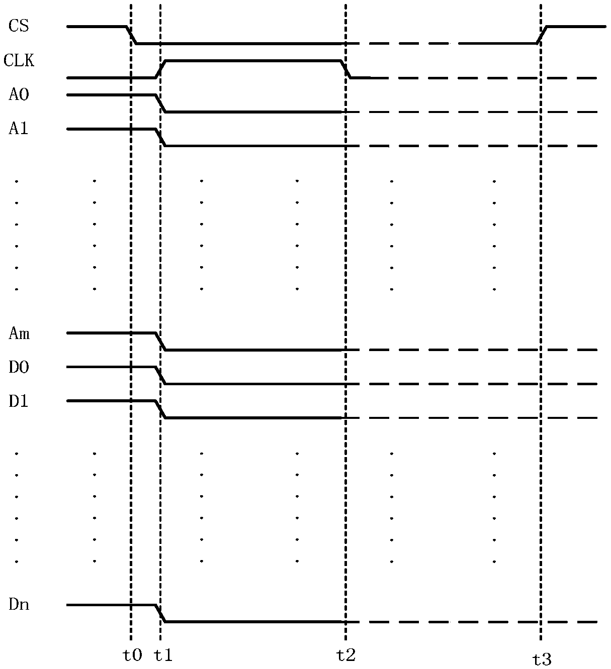
[0078] The second read-write module 73 is used for when the clock signal pin is an ou...


PUM


Abstract

The invention relates to the technical field of communication control, specifically disclosed is a data communication method of Arduino Due and an FPGA. The method comprises the steps of configuring the first level intensities of the communication signal pins of the Arduino Due and the FPGA respectively; when the clock signal pin is an input pin, configuring the level intensity of the chip selection signal pin as second level intensity, and starting to write data from Arduino Due to the FPGA or read data from the FPGA by Arduino Due; if it is detected that the input pin triggers an interrupt response, completing the data writing from the Arduino Due to the FPGA or data reading from the FPGA by the Arduino Due at a time; when the clock signal pin is an output pin, if it is detected that a chip selection signal of the chip selection signal pin drops, starting to write data from the FPGA to the Arduino Due or read data from the Arduino Due by the FPGA; and if the trigger response of the output pin is detected, completing one-time data writing from the FPGA to the Arduino Due or data reading from the Arduino Due by the FPGA. Through the method, the rapid data communication can be carried out between the Arduino Due and the FPGA.

Description

technical field [0001] The present application relates to the technical field of communication control, in particular to a data communication method and system between Arduino Due and FPGA. Background technique [0002] The development of electronic information application technology has driven the rapid development of integrated chips and software tools, making integrated chips based on C / C++, python, Java, verilog HDL and other languages ​​widely used. Among them, C / C++-based ARM, DSP, verilog HDL-based FPGA and its integrated embedded system are widely used in actual signal processing, motion control and other fields. Since Massimo Banzi and others developed Arduino in 2005, there have been many Arduino models such as Arduino Uno, Nano, Mega2560, Due and many other extended hardware platforms such as Arduino GSM Shield, Wireless ProtoShield, WiFi Shield and Motor Shield. Among them, Arduino Due uses AtmelSAM3X8E CPU chip, which is the first Arduino model based on 32-bit ...

Claims


Application Information

Patent Timeline
Patent Type & Authority Applications(China)
IPC IPC(8): G06F13/40G06F13/42
CPCG06F13/4068G06F13/4221G06F13/4282
Inventor 王卫兵张鲁薇王锐王挺峰郭劲
Owner CHANGCHUN INST OF OPTICS FINE MECHANICS & PHYSICS CHINESE ACAD OF SCI
Why Eureka
Try Eureka