Chip used for realizing structure activity relationship indirect in-situ characterization with TEM and manufacturing method thereof

A manufacturing method and chip technology, applied in the preparation of test samples, material analysis using radiation, instruments, etc., can solve problems such as the inability to correlate material structure with material physical and chemical properties

Active Publication Date: 2019-04-26
SHANGHAI INST OF MICROSYSTEM & INFORMATION TECH CHINESE ACAD OF SCI
View PDF7 Cites 5 Cited by
  • Summary
  • Abstract
  • Description
  • Claims
  • Application Information

AI Technical Summary

Problems solved by technology

[0006] In view of the shortcomings of the prior art described above, the purpose of the present invention is to provide a chip for indirect in-situ characterization of TEM structure-activity correlation and its manufacturing method, which is used to solve the problem of material structure and material physicalization that cannot be realized in the prior art. Performance correlation, the problem of in situ characterization of structure-activity correlation

Method used


Image

  • Chip used for realizing structure activity relationship indirect in-situ characterization with TEM and manufacturing method thereof
  • Chip used for realizing structure activity relationship indirect in-situ characterization with TEM and manufacturing method thereof
  • Chip used for realizing structure activity relationship indirect in-situ characterization with TEM and manufacturing method thereof

Examples


Embodiment 1

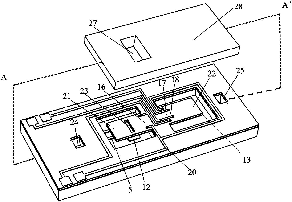
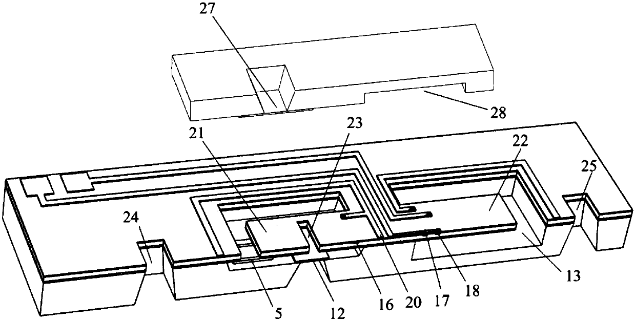
[0085] refer to Figure 1 ~ Figure 4 , this embodiment provides a chip for indirect in situ characterization of TEM structure-activity correlation, the chip includes a main chip and a secondary chip, wherein the main chip includes:

[0086] A detection cantilever beam 22, through which the resonance of the detection cantilever beam 22 is used to detect the mass change of the sample to be measured located on the detection cantilever beam 22;

[0087] The main chip groove 13, the main chip groove 13 is located under the detection cantilever beam 22, and the resonance of the detection cantilever beam 22 is provided by the main chip groove 13 to accommodate the space;

[0088] Observation cantilever beam 21, described observation cantilever beam 21 comprises observation hole 23;

[0089] Main chip window, the main chip window 12 is located below the observation hole 23;

[0090] Air holes, the air holes are located on the outside of the detection cantilever beam 22 and the obser...

Embodiment 2

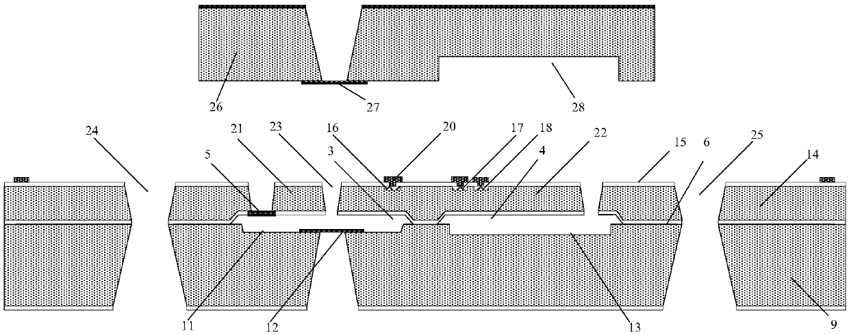
[0114] This embodiment also provides a method for manufacturing a chip for indirect in-situ characterization of TEM structure-activity correlation, the chip includes a main chip and an auxiliary chip, wherein making the main chip includes the following steps:

[0115] Provide the main chip substrate;

[0116] Fabricate a detection cantilever beam, a main chip groove, an observation cantilever beam, a main chip window, and an air hole in the main chip substrate; wherein, the main chip groove is located below the detection cantilever beam, passing through the main chip groove Provide accommodation space for the resonance of the detection cantilever beam; the observation cantilever beam includes an observation hole; the main chip window is located below the observation hole; the air hole is located outside the detection cantilever beam and the observation cantilever beam and runs through The main chip, the air hole includes a main chip air inlet and a main chip air outlet; the re...


PUM

PropertyMeasurementUnit
thicknessaaaaaaaaaa
thicknessaaaaaaaaaa
depthaaaaaaaaaa

Abstract

The invention provides a chip used for realizing structure activity relationship indirect in-situ characterization with a TEM and a manufacturing method thereof. The chip comprises a main chip body and an auxiliary chip body, the main chip body comprises a detection cantilever beam, a main chip body groove, an observing cantilever beam with an observing hole, a main chip body window and an air hole; the auxiliary chip body comprises an auxiliary chip body window used for detecting the quality change of a to-be-detected sample located on the detection cantilever beam through the resonance of the cantilever beam; the main chip body and the auxiliary chip body are arranged oppositely and separately fixed to a TEM sample pole, and a closed space is formed by the main chip body, the auxiliary chip body and the TEM sample pole; the TEM observes the morphology change of the to-be-detected sample located on the observing cantilever beam through the auxiliary chip body window, the observing hole and the main chip body window. Through the chip, indirection in-situ real-time characterization of the morphology change and the quality change can be realized in the TEM, and the chip can be widelyapplied to TEM in-situ characterization of a nanometer material during a gas-solid reaction.

Description

technical field [0001] The invention belongs to the field of TEM in-situ characterization, and relates to a chip for TEM structure-activity correlation indirect in-situ characterization and a manufacturing method thereof. Background technique [0002] So far, the research of nanomaterials has achieved rich results, how to make the research results of nanomaterials to be functionalized and widely used has become the main problem at present. To achieve this breakthrough, correlating the nanostructure with its properties and establishing a clear structure-activity relationship is an effective way to solve the problem. [0003] In the observation of nanostructures, methods such as transmission electron microscopy (TEM), scanning electron microscopy (SEM), and scanning probe microscopy (SPM) have been widely used, and the resolution can reach the single-atom level. However, these methods are mainly limited to the characterization of nanostructure and morphology, and it is diffic...

Claims


Application Information

Patent Timeline
Patent Type & Authority Applications(China)
IPC IPC(8): G01N5/00G01N23/04G01N1/28H01J37/26
CPCG01N1/28G01N5/00G01N23/04H01J37/261
Inventor 李昕欣于海涛许鹏程李伟王雪晴李明
Owner SHANGHAI INST OF MICROSYSTEM & INFORMATION TECH CHINESE ACAD OF SCI
Why Eureka
Try Eureka