Method for preparing AgBiS2 semiconductor film
A semiconductor and thin film technology, which is applied in the field of AgBiS2 semiconductor thin film preparation, can solve the problems that it is difficult to deposit a film with sufficient thickness, not completely absorb photon energy, and limit the application of photovoltaic conversion, so as to improve photovoltaic performance and accurately control the composition , The effect of low equipment requirements
- Summary
- Abstract
- Description
- Claims
- Application Information
AI Technical Summary
Problems solved by technology
Method used
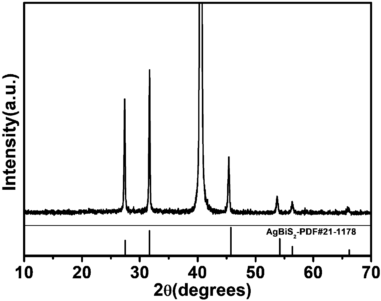
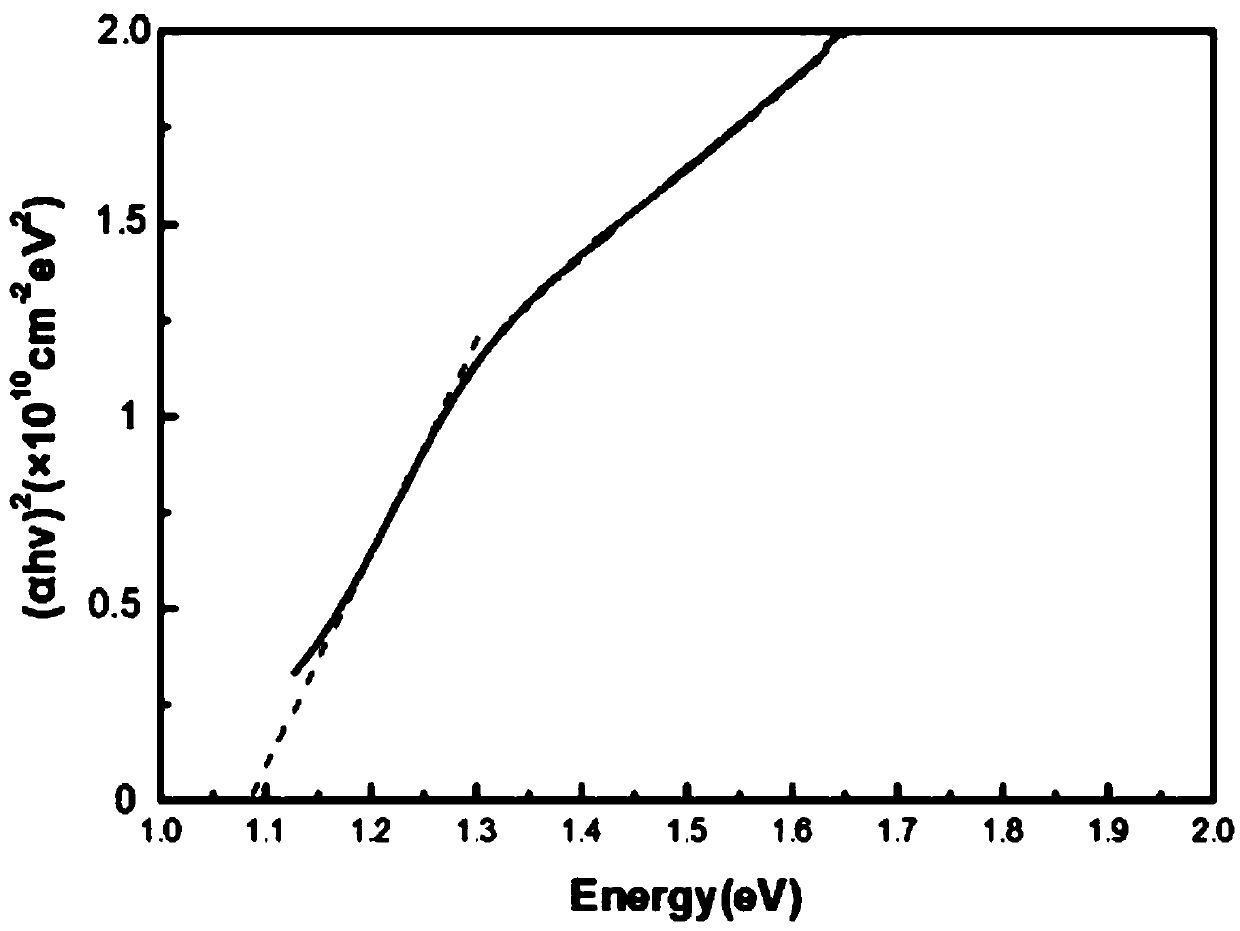
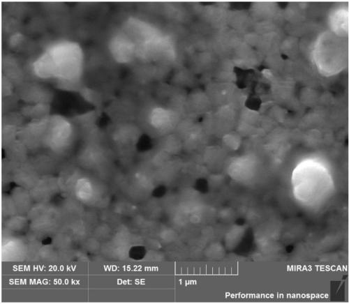
Image

Examples
Embodiment 1
[0038] Dissolve silver nitrate in 10 ml of pure water to obtain a 0.25 mol / L silver nitrate solution (stir at room temperature for 30 minutes to obtain a colorless and clear solution). At the same time, bismuth nitrate pentahydrate was added to 10 ml of acetic acid solution to obtain a 0.25 mol / L bismuth source solution (stir at 50° C. for 30 minutes to obtain a colorless and clear solution).
[0039] Then silver nitrate solution and bismuth source solution were mixed, heated to 60°C, 1.903g of thiourea was added rapidly, and fully stirred for 30min to obtain a yellow clear solution without precipitation. After the above solution was cooled, 0.5ml of diethanolamine and 0.5ml of triethanolamine were added dropwise, and stirred at room temperature for five minutes to obtain a precursor solution. The viscosity of the precursor solution was significantly higher than that without additives.
[0040] Then the prepared AgBiS 2 The precursor solution was spin-coated on Mo glass, pre-...
Embodiment 2
[0044] Dissolve silver fluoride in 30ml pure water to obtain a 0.5mol / L silver source solution. At the same time, bismuth chloride was added to 30 ml of dilute nitric acid solution to obtain a 0.25 mol / L bismuth source solution (stirred at 50° C. for 30 minutes to obtain a colorless and clear solution).
[0045] Then mix the silver source solution and the bismuth source solution, heat to 50°C, quickly add 4.5672g thiourea, and fully stir for 30min to obtain a yellow clear solution without precipitation.
[0046] After the above solution was cooled, 2ml of ethanolamine was added dropwise, and stirred at room temperature for five minutes to obtain a precursor solution, which was set aside. Then the prepared AgBiS 2 The precursor solution was squeegee-coated on the FTO conductive glass substrate and white glass (for UV testing), pre-fired at 270°C between each two squeegee coatings, and spin-coated 10 times to complete the AgBiS 2 Spin-coating of prefabricated layers, tested, A...
Embodiment 3
[0050] Dissolve silver nitrate in 50 ml of pure water to obtain a 2 mol / L silver nitrate solution (stir at room temperature for 60 minutes to obtain a colorless and clear solution). At the same time, bismuth nitrate pentahydrate was added to 70 ml of acetic acid solution to obtain a 2 mol / L bismuth source solution (stirred at 80° C. for 60 minutes to obtain a colorless and clear solution).
[0051] Then silver nitrate solution and bismuth source solution were mixed, heated to 40°C, 28g of thiourea was added rapidly, and fully stirred for 30min to obtain a yellow clear solution without precipitation. After the above solution was cooled, 2ml of ethanol and 2ml of triethanolamine were added dropwise, and stirred for five minutes at room temperature to obtain a precursor solution. The viscosity of the precursor solution was significantly higher than that without additives.
[0052] Then the prepared AgBiS 2 The precursor solution was drop-coated on two Mo conductive glass substra...
PUM
| Property | Measurement | Unit |
|---|---|---|
| Thickness | aaaaa | aaaaa |
| Thickness | aaaaa | aaaaa |
| Size | aaaaa | aaaaa |
Abstract
Description
Claims
Application Information
 - R&D
- Intellectual Property
- Life Sciences
- Materials
- Tech Scout
- Unparalleled Data Quality
- Higher Quality Content
- 60% Fewer Hallucinations
Browse by: Latest US Patents, China's latest patents, Technical Efficacy Thesaurus, Application Domain, Technology Topic, Popular Technical Reports.
© 2025 PatSnap. All rights reserved.Legal|Privacy policy|Modern Slavery Act Transparency Statement|Sitemap|About US| Contact US: help@patsnap.com