A multifunctional communication circuit board testing device

A technology for testing devices and circuit boards, which is applied in printed circuit testing, electronic circuit testing, measuring device casings, etc., can solve problems such as reduced testing efficiency, poor stability of testing mechanisms, and complicated steps, so as to improve testing efficiency and ensure stability , the effect of improving accuracy

Active Publication Date: 2021-08-06
安徽米兰电子科技有限公司
View PDF9 Cites 0 Cited by
  • Summary
  • Abstract
  • Description
  • Claims
  • Application Information

AI Technical Summary

Problems solved by technology

[0002] With the development of electronic products in the direction of miniaturization, multi-function, portability and high performance, circuit boards, which are the main components of electronic products, are also evolving in the direction of high density, multi-layer and fine pitch, which constitutes a significant impact on the circuit board manufacturing industry. If the defective products cannot be screened out in time during the manufacturing process, it will inevitably increase the scrap rate of the product, which will increase the cost of the downstream process
Therefore, it is necessary to improve the testing technology and adopt appropriate testing methods to improve product testing efficiency. The existing circuit board testing device has certain deficiencies in the process of use, and the circuit board cannot be replaced well, and the steps are relatively complicated. , the test efficiency is relatively low, and it is believed that it will be further improved in the future to meet the different needs of use and thus be more widely used;
[0003] The existing circuit board testing device has certain disadvantages in the process of use. It cannot test multiple circuit boards at the same time, and the replacement of circuit boards is more complicated, which greatly reduces the test efficiency. It cannot test different types of circuit boards. For testing, the applicability is not strong, the circuit board cannot be well fixed in multiple directions, and the overall stability of the testing mechanism is poor, which affects the testing accuracy

Method used


Image

  • A multifunctional communication circuit board testing device
  • A multifunctional communication circuit board testing device
  • A multifunctional communication circuit board testing device

Examples


Embodiment Construction

[0027] The technical solutions in the embodiments of the present invention will be clearly and completely described below in conjunction with the embodiments of the present invention. Apparently, the described embodiments are only some of the embodiments of the present invention, not all of them. Based on the embodiments of the present invention, all other embodiments obtained by persons of ordinary skill in the art without creative efforts fall within the protection scope of the present invention.

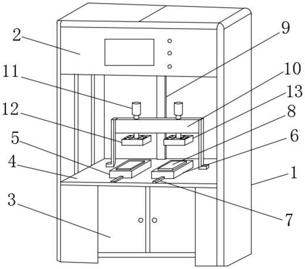
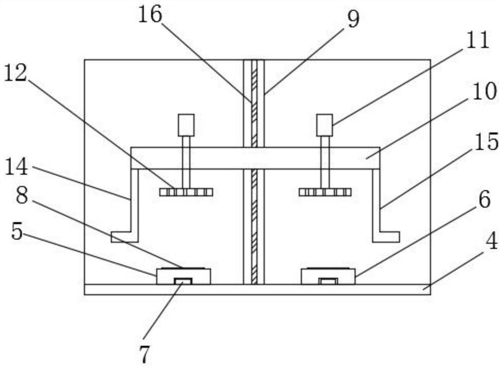
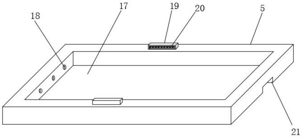
[0028] Such as Figure 1-5 As shown, a multifunctional communication circuit board testing device includes a device frame assembly 1, a top plate 2 is installed on the top of the device frame assembly 1, and an electric box 3 is installed on the bottom of the device frame assembly 1. A test platform 4 is installed on the upper end of the box 3, and two groups of slide bars 7 are arranged in parallel on the surface of the upper end of the test platform 4, and a left load plate 5 an...


PUM


Abstract

The invention discloses a multifunctional communication circuit board testing device, which includes a device frame assembly, a top plate is installed on the top of the device frame assembly, an electric box is installed on the bottom of the device frame assembly, and a test box is installed on the upper end of the electric box. Two sets of slide bars are arranged in parallel on the upper surface of the test platform, and a left load plate and a right load plate are slidably installed on the two sets of slide bars respectively, and circuit boards are arranged on the upper ends of the left load plate and the right load plate , a supporting slide plate is installed between the top plate and the test platform near the middle of the rear end; the present invention can perform functional tests on different types of circuit boards, has strong applicability, realizes simultaneous testing of two groups of circuit boards, and is convenient for staff The circuit board is replaced to improve the test efficiency, and the circuit board can be fixed horizontally and vertically to ensure its overall stability, thereby improving the accuracy of the test.

Description

technical field [0001] The invention belongs to the technical field of circuit board testing, and in particular relates to a testing device, in particular to a multifunctional communication circuit board testing device. Background technique [0002] With the development of electronic products in the direction of miniaturization, multi-function, portability and high performance, circuit boards, which are the main components of electronic products, are also evolving in the direction of high density, multi-layer and fine pitch, which constitutes a significant impact on the circuit board manufacturing industry. If the defective products cannot be screened out in time during the manufacturing process, it will inevitably increase the scrap rate of the product, which will increase the cost of the downstream process. Therefore, it is necessary to improve the testing technology and adopt appropriate testing methods to improve product testing efficiency. The existing circuit board tes...

Claims


Application Information

Patent Timeline
Patent Type & Authority Patents(China)
IPC IPC(8): G01R31/28G01R1/04
CPCG01R31/2808
Inventor 聂润华
Owner 安徽米兰电子科技有限公司
Why Eureka
Try Eureka