Packaging method and packaging device

A packaging method and technology for packaging devices, which are applied in the fields of electrical solid device, semiconductor device, semiconductor/solid device manufacturing, etc., can solve the problems of high cost and time cost of prefabricated solder paste process, reduce process cost and time cost, and reduce welding cost. Defects, the effect of reducing the placement time

Inactive Publication Date: 2019-05-03
NANTONG FUJITSU MICROELECTRONICS
View PDF4 Cites 0 Cited by
  • Summary
  • Abstract
  • Description
  • Claims
  • Application Information

AI Technical Summary

Problems solved by technology

[0003] The inventors of the present application found in the long-term research process that the above-mentioned process needs to prefabricate solder paste on the metal bumps / metal studs of the chip, and the process cost and time cost of prefabricating solder paste are relatively high

Method used


Image

  • Packaging method and packaging device
  • Packaging method and packaging device
  • Packaging method and packaging device

Examples


Embodiment Construction

[0026] The following will clearly and completely describe the technical solutions in the embodiments of the present application with reference to the drawings in the embodiments of the present application. Obviously, the described embodiments are only some of the embodiments of the present application, not all of them. Based on the embodiments in the present application, all other embodiments obtained by persons of ordinary skill in the art without making creative efforts belong to the protection scope of the present application.

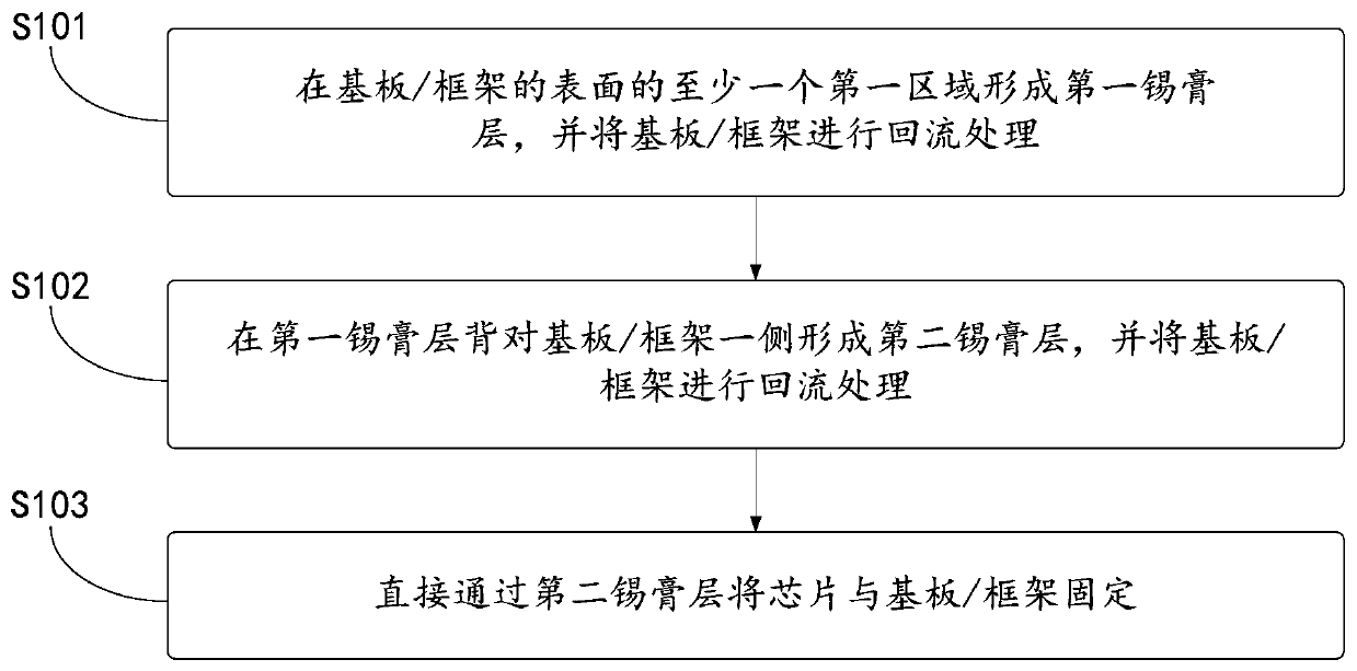
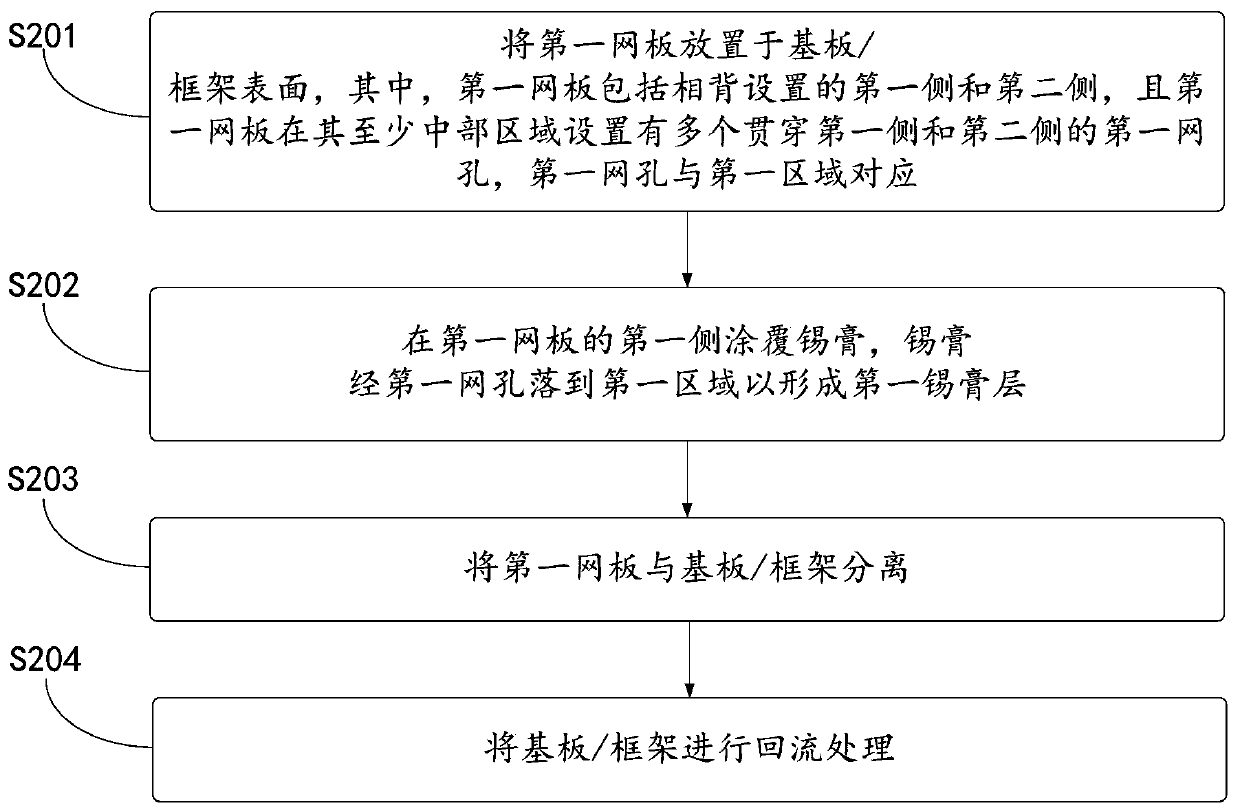
[0027] see figure 1 , figure 1 It is a schematic flow chart of an implementation mode of the packaging method of the present application. The packaging method provided in the present application includes:

[0028] S101: Form a first solder paste layer on at least one first region of the surface of the substrate / frame, and perform a reflow process on the substrate / frame.

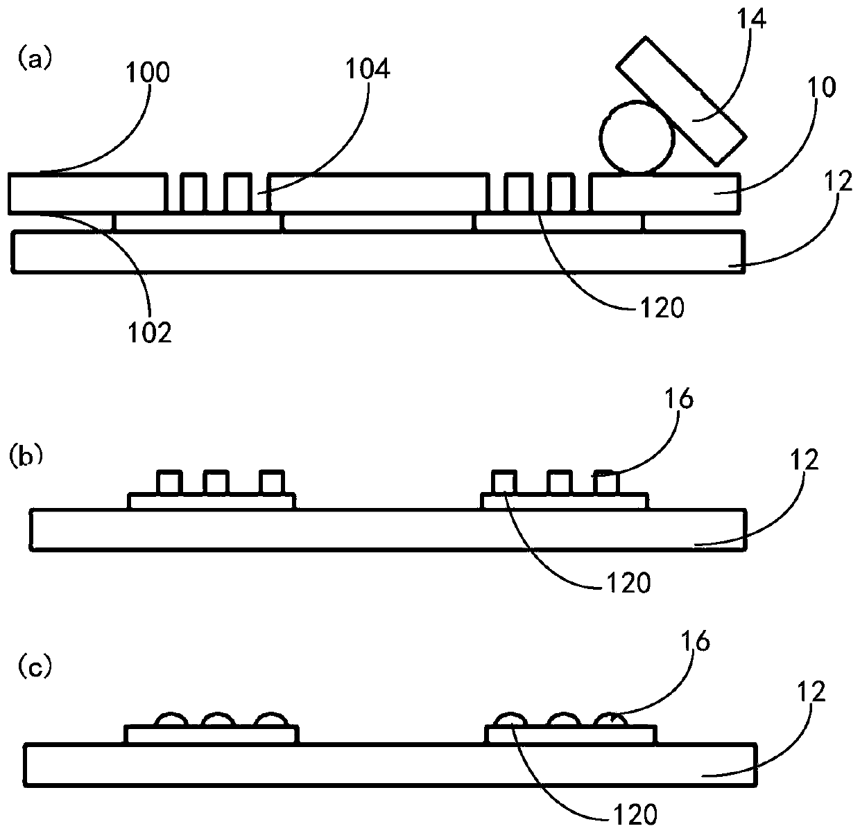
[0029] Specifically, in the field of semiconductor packaging technology, the...


PUM


Abstract

The present application discloses a packaging method and a packaging device. The packaging method comprises forming a first solder paste layer in at least one first region on the surface of a substrate / frame, and performing a reflow process on the substrate / frame; forming a second solder paste layer on a side of the first solder paste layer away from the substrate / frame, and performing a reflow process on the substrate / frame; directly fixing a chip to the substrate / frame through the second solder paste layer. The method can directly fix the chip to the substrate / frame without prefabricating the solder paste on the chip.

Description

technical field [0001] The present application relates to the field of packaging technology, in particular to a packaging method and a packaging device. Background technique [0002] In the field of semiconductor packaging technology, the commonly used method for fixing the chip to the substrate / frame includes: forming solder paste on the metal bump / metal post of the chip, and then placing the end of the chip with the solder paste on the solder flux In the groove of the chip, so that the flux is attached to the metal bumps / posts of the chip; the end of the chip with the flux is in contact with the surface of the substrate / frame; the chip and the substrate / frame are reflowed as a whole, and then the chip Fixed to substrate / frame surface. [0003] The inventors of the present application have discovered during long-term research that the above-mentioned process needs to prefabricate solder paste on the metal bumps / pillars of the chip, and the process cost and time cost of pre...

Claims


Application Information

Patent Timeline
IPC IPC(8): H01L21/60H01L23/488
CPCH01L2224/16225H01L2224/81
Inventor 沈海军
Owner NANTONG FUJITSU MICROELECTRONICS
Why Eureka
Try Eureka