An integrated module and power device

A technology for integrating modules and devices, applied in semiconductor devices, electro-solid devices, semiconductor/solid-state device components, etc., it can solve the problems of component aging failure, component damage, large current load, etc., and achieve high mold clamping and packaging pressure. , reduce parasitic inductance, reduce the effect of path and area

Active Publication Date: 2022-04-29
FOSHAN NATIONSTAR OPTOELECTRONICS CO LTD
View PDF8 Cites 0 Cited by
  • Summary
  • Abstract
  • Description
  • Claims
  • Application Information

AI Technical Summary

Problems solved by technology

[0003] On the one hand, with the miniaturization of components in the inverter module, due to frequent circuit switching, large current load, and serious heat generation, it is easy to cause aging and failure of components. Therefore, it is necessary to optimize the structure of components involved in inverter conversion Perform thermal optimization
Existing products have adopted double-sided packaging to enhance the heat dissipation capability of components, but the specific process involves double-sided molded packaging of components, which may easily lead to damage to components

Method used


Image

  • An integrated module and power device
  • An integrated module and power device
  • An integrated module and power device

Examples


Embodiment 1

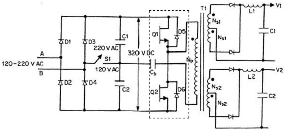
[0063] In the same device group, the cathode of the diode is bonded to the module substrate, and the drain of the switch transistor is bonded to the module substrate. Specifically, the device group to which this embodiment is applied is the first device group 10 . Specifically, in the embodiment of the present invention, the module substrate 3 is used as the O pole, corresponding to the image 3 In the circuit structure shown, the cathode of the first diode 101 is bonded to the second connection surface layer 312 of the module substrate, and the drain D01 of the first switch tube 102 is bonded to the module substrate 3 On the first connection surface layer 311 ; the gate G01 and the source S01 of the first switch tube 102 face away from the module substrate 3 .

Embodiment 2

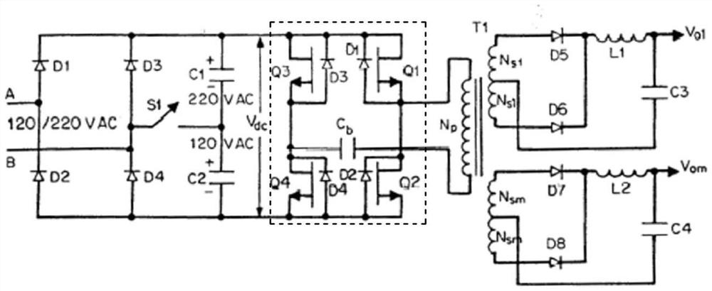
[0065] In the same group of devices, the anode of the diode is bonded on the module substrate, and the source of the switch tube is bonded on the module substrate, and the module substrate corresponds to the switch The gate position of the tube is provided with a grid connector; the start and end of the grid connector pass through the two connection surfaces of the module substrate respectively, and the start end of the grid connector is connected to the switch tube the gate bonding; the connection remains insulated from the module substrate. Specifically, the device group to which this embodiment is applied is the second device group 20 .

[0066] Specifically, the module substrate 3 is used as the O pole, the anode of the second diode 201 is bonded to the first connection surface layer 311 of the module substrate 3, and the source S02 of the second switch tube 202 is bonded to combined on the second connection surface layer 312 of the module substrate 3; the module substrat...


PUM


Abstract

The invention provides an integrated module, which includes a module substrate and several device groups; the device group includes two devices, and the two devices are respectively a switch tube and a diode; the module substrate includes a first connection surface layer and a second connection surface electrically connected surface layer; in the same group of device groups, the cathode of the diode is bonded on the first connection surface layer or the second connection surface layer, and the drain of the switch tube is bonded on the first connection surface layer or the second connection surface layer; or in the same group In the device group, the anode of the diode is bonded on the first connection surface layer or the second connection surface layer, and the source electrode of the switch tube is bonded on the module substrate, and the module substrate is provided with a gate at a position corresponding to the gate of the switch tube. pole connector; the start of the grid connector is bonded to the grid of the switch tube, and the end of the grid connector passes through the module substrate; the grid connector is kept insulated from the module substrate. The integrated module has a wide range of applications and is highly convenient to use. In addition, the invention also provides a power device.

Description

technical field [0001] The invention relates to the field of electronic devices, in particular to an integrated module and a power device. Background technique [0002] figure 1 A schematic diagram of the circuit structure of a half-bridge inverter power conversion circuit is shown, figure 2 A schematic circuit structure diagram of a full-bridge inverter power conversion circuit is shown. The switch inverter modules widely used in power conversion circuits are half-bridge inverter modules and full-bridge inverter modules, combined with the accompanying drawings figure 1 and attached figure 2 The structure shown (the area surrounded by the dotted line box) is only for the number of components, the number of components included in the inverter module in the full-bridge inverter power conversion circuit (the number of switching tubes Q and diodes D in the dotted line box) It is twice the number of components (switch tube Q and diode D in the dashed box) included in the in...

Claims


Application Information

Patent Timeline
Patent Type & Authority Patents(China)
IPC IPC(8): H01L23/31H01L25/07H01L23/48
CPCH01L23/3121H01L25/071H01L23/481
Inventor 杨宁谢健兴袁毅凯
Owner FOSHAN NATIONSTAR OPTOELECTRONICS CO LTD
Why Eureka
Try Eureka