


Quick Research
Generate reliable direction feasibility study reports for your R&D in just a few steps.

Technical Q&A
Discover and master advanced knowledge NOW. Basics, ideas, possibilities, all at once.

Find Solutions
As an expert in R&D theories, this can generate solutions to your technical problems instantly.

Evaluate Feasibility
Analyze your overall solution with one click, know your potential R&D risks in advance.

Monitor Landscape
Get weekly tech updates, stay abreast of the latest tech innovations and key insights.
Semiconductor nanowire laser device with rapid wavelength tuning
A semiconductor and nanowire technology, applied in the laser field, can solve problems such as low repeatability of operation, low tuning speed, and irreversible tuning, and achieve the effects of fast tuning, precise control, and adjustable time delay
- Summary
- Abstract
- Description
- Claims
- Application Information
AI Technical Summary
Problems solved by technology
Method used
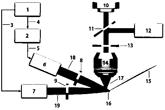
Image

Examples
Embodiment 1
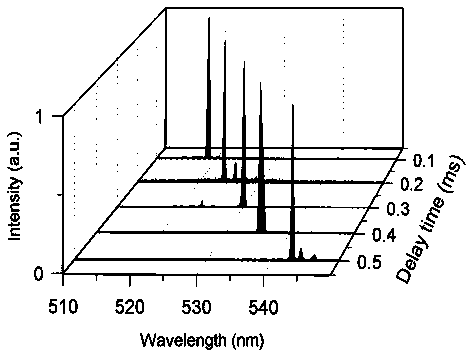
[0027] In this embodiment, the CdS semiconductor nanowires are suspended in the air, and a 355 nm pulsed laser is used to pump the CdS semiconductor nanowires to achieve laser output. 2 The pulsed laser (laser output wavelength: 10.6 μm) performs rapid temperature control on the CdS semiconductor nanowires to realize the rapid tuning of the output wavelength of the semiconductor nanowire laser. The 355 nm pulsed laser and CO 2 The output repetition frequency of the pulsed laser is equal to 200 Hz, the pulse width of the 355 nm pulsed laser is 3.5 ns, and the pump power density is 10 kW / cm 2 , CO 2 The pulse width of the pulsed laser is 500 μs, and the 355 nm pulsed laser with CO 2 The pulse time delay between pulsed lasers is τ 1 .
[0028] figure 2 Shown is the laser output wavelength versus delay τ for a CdS semiconductor nanowire with a diameter of 400 nm and a length of 10 μm 1 Graphs of results that vary as a function of change. figure 2 It can be seen that the ti...
Embodiment 2
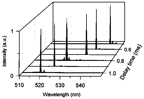
[0030] In this embodiment, the CdS semiconductor nanowires are suspended in the air, and a 355 nm pulsed laser is used to pump the CdS semiconductor nanowires to achieve laser output. 2 A pulsed laser (laser output wavelength: 10.6 μm) performs rapid temperature control on CdS semiconductor nanowires to realize rapid tuning of the output wavelength of the semiconductor nanowire laser. A 355 nm pulsed laser and CO 2 The output repetition frequency of the pulsed laser is equal to 200 Hz, the pulse width of the 355 nm pulsed laser is 3.5 ns, and the pump power density is 10 kW / cm 2 , CO 2 The pulse width of the pulsed laser is 500 μs, and the 355 nm pulsed laser with CO 2 The pulse time delay between pulsed lasers is τ 2 .
[0031] image 3 Shown is the laser output wavelength versus delay τ for a CdS semiconductor nanowire with a diameter of 500 nm and a length of 12 μm 2 Graphs of results that vary as a function of change. It can be seen from the figure that the time dela...
Embodiment 3
[0033] In this example, the CdS semiconductor nanowires are suspended in the air, and the nanowires are pumped by a 355 nm pulsed laser to achieve laser output. 2 A pulsed laser (laser output wavelength: 10.6 μm) performs rapid temperature control on CdS semiconductor nanowires to realize rapid tuning of the output wavelength of the semiconductor nanowire laser. A 355 nm pulsed laser and CO 2 The output repetition frequency of the pulsed laser is equal to 200 Hz, the pulse width of the 355 nm pulsed laser is 3.5 ns, and the pump power density is 10kW / cm 2 , CO 2 The pulse width of the pulsed laser is 500 μs, and the 355 nm pulsed laser with CO 2 The pulse time delay between pulsed lasers is τ 3 .
[0034] Figure 4 Shown is the laser output wavelength versus delay τ for a CdS semiconductor nanowire with a diameter of 500 nm and a length of 13 μm 3 Graphs of results that vary as a function of change. Figure 4 It can be seen in the time delay τ 3 in the range of 1.5-4.5 ...
PUM
 Abstract
Description
Claims
Application Information
 - R&D Engineer
- R&D Manager
- IP Professional
- Industry Leading Data Capabilities
- Powerful AI technology
- Patent DNA Extraction
Browse by: Latest US Patents, China's latest patents, Technical Efficacy Thesaurus, Application Domain, Technology Topic, Popular Technical Reports.
© 2024 PatSnap. All rights reserved.Legal|Privacy policy|Modern Slavery Act Transparency Statement|Sitemap|About US| Contact US: help@patsnap.com