Magnetic isolation drive circuit

A driving circuit and magnetic isolation technology, applied in the direction of electrical components, adjusting electrical variables, instruments, etc., can solve the problems of large energy consumption and untimely opening of MOS tubes

Active Publication Date: 2019-05-10
MORNSUN GUANGZHOU SCI & TECH
View PDF10 Cites 5 Cited by
  • Summary
  • Abstract
  • Description
  • Claims
  • Application Information

AI Technical Summary

Problems solved by technology

The delayed turn-off of the bipolar transistor Q1 leads to the untimely turn-on of the driven MOS tube, which is an important shortcoming of this type of circuit
and Figure 1-4 When the positive driving pulse signal of the next cycle comes, the input capacitance of the P-channel field effect transistor Q2 must be discharged through R5 before it can exit the saturation zone. After Q2 exits the saturation zone, the MOS tubes connected to the C and D terminals Or the IGBT will be turned on. During this period, due to the small voltage drop of D2, the induced voltage of Ns1 is short-circuited through D2, R6 and R7, and the energy consumption is large.

Method used


Image

  • Magnetic isolation drive circuit
  • Magnetic isolation drive circuit
  • Magnetic isolation drive circuit

Examples


no. 1 example

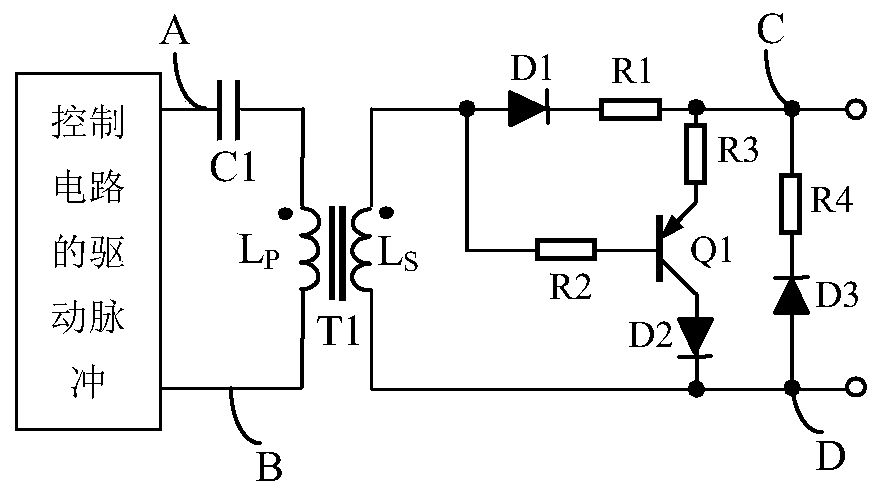
[0037] see figure 2 , figure 2 It is a schematic diagram of the magnetic isolation driving circuit of the first embodiment of the present invention.

[0038] The magnetic isolation driving circuit of this embodiment includes a first input terminal Si1, a second input terminal Si2, a first output terminal So1, a second output terminal So2, a switch tube Q10, a diode D10, a TVS diode, a transformer B, and a primary winding N P , secondary winding N S , diode D11, diode D12, resistor R11, resistor R12 and transistor Q11;

[0039] The TVS diode is a transient suppression diode TVS, which is Transient Voltage Suppressor in English, and is essentially a Zener diode that can withstand high power instantaneously. Because, in the technical solution of this application, the use of a Zener tube also achieves the purpose of the invention, that is, in this application, TVS diodes include Zener diodes, and also include such "zener diodes" that use the emitter or collector junctions in ...

no. 2 example

[0051] see image 3 , image 3 It is a schematic diagram of a magnetic isolation driving circuit according to the second embodiment of the present invention.

[0052] The magnetic isolation driving circuit of this embodiment includes a first input terminal Si1, a second input terminal Si2, a first output terminal So1, a second output terminal So2, a switch tube Q10, a diode D10, a TVS diode, a transformer B, and a primary winding N P , secondary winding N S , diode D11, resistor R11, resistor R12 and transistor Q11;

[0053] The positive pole of the external voltage source Vs is connected to the first input terminal Si1, the negative pole of the voltage source Vs is connected to the second input terminal Si2, the anode of the TVS diode is connected to the first input terminal Si1, the cathode of the TVS diode is connected to the cathode of the diode D10, and the anode of the diode D10 The drain of the switching tube Q10 is connected, the source of the switching tube Q10 is ...

no. 3 example

[0061] see Figure 4 , Figure 4 It is a schematic diagram of the magnetic isolation driving circuit of the third embodiment of the present invention.

[0062] The magnetic isolation driving circuit of this embodiment includes a first input terminal Si1, a second input terminal Si2, a first output terminal So1, a second output terminal So2, a switch tube Q10, a diode D10, a TVS diode, a transformer B, and a primary winding N P , secondary winding N S , diode D11, diode D12, diode D13, resistor R11, capacitor C11 and transistor Q11;

[0063] The positive pole of the external voltage source Vs is connected to the first input terminal Si1, the negative pole of the voltage source Vs is connected to the second input terminal Si2, the anode of the TVS diode is connected to the first input terminal Si1, the cathode of the TVS diode is connected to the cathode of the diode D10, and the anode of the diode D10 The drain of the switching tube Q10 is connected, the source of the switch...


PUM


Abstract

The present invention discloses a magnetic isolation drive circuit, comprising a first input end, a second input end, a first output end, a second output end, a switch tube Q10, a diode D10, a TVS diode, a transformer B, a primary winding, a secondary winding, and an acceleration switch-off circuit at the secondary side, wherein the acceleration switch-off circuit includes at least one switch tubeQ11, the positive electrode of the TVS diode is connected to the first input end, the negative electrode of the TVS diode is connected to the negative electrode of the diode D10, the positive electrode of the diode D10 is connected to a drain electrode of the switch tube Q10, and a source electrode of the switch tube Q10 is connected to the second input end, and two ends of the primary winding are respectively connected to the first input end and the second input end. In first few cycles of the circuit, when a primary side MOS transistor is turned off, a primary voltage of the transformer isclamped to a set value by the TVS, and the secondary side can generate a sufficiently large induced voltage and a reverse current to drive operation of the acceleration switch-off circuit, to achievea fast switch-off of a driven power switch component, so that the circuit is no longer out of control in the first few cycles.

Description

technical field [0001] The invention relates to a driving circuit of a power switching device, in particular to a magnetic isolation driving circuit of a power switching device. Background technique [0002] Power switching devices occupy a core position in power electronic devices, and their reliable operation is the basis for the normal operation of the entire device. The driving circuit of the power switching device is the interface between the main circuit and the control circuit, and is an important part of the power electronic device. It has a great influence on the performance of the whole device, and its function is to amplify the driving pulse signal output by the control circuit enough to drive the power switching device and perform necessary isolation. In short, the basic task of the drive circuit is to convert the drive pulse signal from the control circuit into a signal that can be added between the control terminal of the power switching device and the outflow...

Claims


Application Information

Patent Timeline
Patent Type & Authority Applications(China)
IPC IPC(8): H02M3/335
Inventor 王保均
Owner MORNSUN GUANGZHOU SCI & TECH
Why Eureka
Try Eureka