Semiconductor device test system and test method thereof

A test system and semiconductor technology, which is applied in the direction of single semiconductor device testing, instrumentation, measuring electricity, etc., can solve the problem of not designing the test circuit, etc., and achieve the effect of easy disassembly, detachable connection, and convenient connection

Pending Publication Date: 2020-04-03
HEFEI KEWELL POWER SYST CO LTD
View PDF1 Cites 10 Cited by
  • Summary
  • Abstract
  • Description
  • Claims
  • Application Information

AI Technical Summary

Problems solved by technology

However, it did not design a specific test circuit and test system structu

Method used


Image

  • Semiconductor device test system and test method thereof
  • Semiconductor device test system and test method thereof
  • Semiconductor device test system and test method thereof

Examples


Embodiment 1

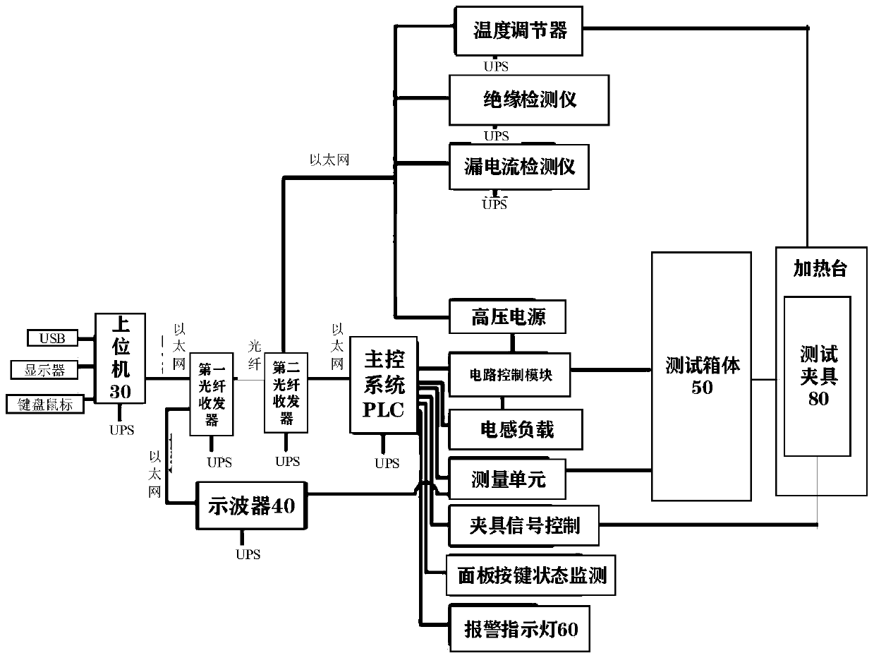
[0069] like figure 1 and Figure 13 As shown, a semiconductor device testing system includes a host computer 30, an oscilloscope 40, a main control system PLC, a circuit control module, a test box 50, a UPS power supply, a first optical fiber transceiver, a second optical fiber transceiver, and a temperature regulator , an insulation detector, a leakage current detector, a high voltage power supply, an inductive load, a measuring unit and an alarm indicator 60, the circuit control module includes a main circuit unit, a gate drive unit, a pulse digital power amplifier unit, a high voltage generating unit and a current sampling unit, wherein the pulse digital power amplifier unit, the high voltage generation unit and the current sampling unit adopt the circuit structure of the prior art. An automated tooling 70 is set in the test box 50, such as Image 6 As shown, the test piece 6 is placed on the automated tooling 70, and the test fixture 80 is set directly above the test pie...

Embodiment 2

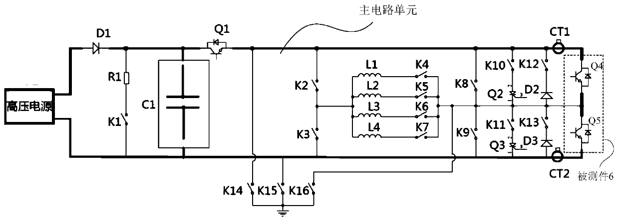
[0075] The difference between Embodiment 2 of the present invention and Embodiment 1 is that a specific implementation manner of the main circuit unit is provided, which will be described in detail below.

[0076] like figure 2 As shown, the main circuit unit includes a high-voltage power supply, sequentially numbered switch K2 to switch K11, thyristor Q2, thyristor Q3, inductor L1, inductor L2, inductor L3, inductor L4, anti-reverse diode D1, resistor R1, switch K1, Supporting capacitor C1, current limiting transistor Q1, diode D2, diode D3, switch K12, switch K13, current sensor CT1, current sensor CT2, switch K14, switch K15 and switch K16, the device under test 6 includes a first transistor Q4 and the second transistor Q5.

[0077] The positive pole of the anti-reverse diode D1 is connected to the positive pole of the high-voltage power supply, one end of the resistor R1 is connected to the negative pole of the anti-reverse diode D1, the other end of the resistor R1 is c...

Embodiment 3

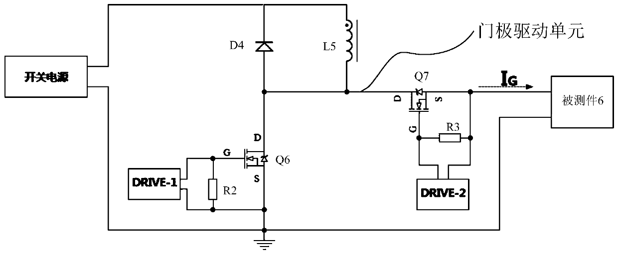
[0089] like image 3 As shown, the difference between Embodiment 3 and Embodiment 1 of the present invention lies in the provision of a specific implementation manner of the gate drive unit, which will be described in detail below.

[0090] The gate drive unit includes a switching power supply, a transistor Q6, a transistor Q7, a diode D4, an inductor L5, a resistor R2, a resistor R3, a first driving module DRIVE-1 and a second driving module DRIVE-2, and the switching power supply is respectively connected to The negative pole of the diode D4 and the source pole of the transistor Q6, the positive pole of the diode D4 is connected to the drain pole of the transistor Q6; The anode of the diode D4; the drain of the transistor Q7 is connected to the opposite end of the inductance L5, the source of the transistor Q7 is connected to the device under test 6, and the sources of the device under test 6 and the transistor Q6 are all grounded;

[0091] The first drive module DRIVE-1 is...


PUM


Abstract

The invention discloses a semiconductor device test system and a test method thereof. The test system comprises an upper computer, an oscilloscope, a main control system PLC, a circuit control moduleand a test box body. An automatic tool is arranged in the test box body, a tested piece is placed on the automatic tool, and a test fixture is arranged right above the tested piece. The automatic toolcomprises a driving device, the driving device drives the automatic tool to move so as to drive the tested piece to be connected with the test fixture, and the main control system PLC is connected with the test box body, the test fixture, a main circuit unit and a gate pole driving unit. The upper computer is connected with the oscilloscope, and the oscilloscope is connected with the test box body. The advantages of the present invention are that the semiconductor device test system with a specific testing circuit and a testing system structure is designed, the theory is combined with the practice, and all devices in the system are matched with one another to test the semiconductor device.

Description

technical field [0001] The invention relates to the field of semiconductor device characteristic testing, and more specifically relates to a semiconductor device testing system and a testing method thereof. Background technique [0002] IGBT is a mainstream semiconductor switching device widely used in modern medium and high-power converters. Its switching characteristics determine the switching loss, power density, device stress and electromagnetic compatibility of the device, and directly affect the performance of the converter. The characteristic research of IGBT includes static characteristic research and dynamic characteristic research, the static characteristic can often be obtained from the datasheet (data sheet), and the dynamic characteristic needs to be measured manually. In the current national standard and IEC (International Electrotechnical Commission, International Electrotechnical Commission) standard, the measurement of dynamic characteristics is based on the...

Claims


Application Information

Patent Timeline
IPC IPC(8): G01R31/26
CPCG01R31/2603
Inventor 韩正王刚朱国军唐德平
Owner HEFEI KEWELL POWER SYST CO LTD
Why Eureka
Try Eureka