A compact nested inductor structure based on through-silicon vias and its preparation method

A technology of through-silicon vias and nesting, which is applied in the field of compact nested inductance structures based on through-silicon vias and its preparation, can solve problems such as increasing the inductance value, increasing the number of rings, and affecting integration density, so as to improve the inductance value , increase inductance density, reduce the effect of occupied area

Active Publication Date: 2020-08-21
XIDIAN UNIV
View PDF2 Cites 0 Cited by
  • Summary
  • Abstract
  • Description
  • Claims
  • Application Information

AI Technical Summary

Problems solved by technology

Due to the existence of dead zones in the manufacture and design of TSVs, while increasing the number of loops to increase the inductance value, the dead zone area of ​​this unidirectional transmission TSV inductance is also increasing. In high-density radio frequency In circuit transmission, it affects the overall integration density

Method used


Image

  • A compact nested inductor structure based on through-silicon vias and its preparation method
  • A compact nested inductor structure based on through-silicon vias and its preparation method
  • A compact nested inductor structure based on through-silicon vias and its preparation method

Examples


Embodiment 1

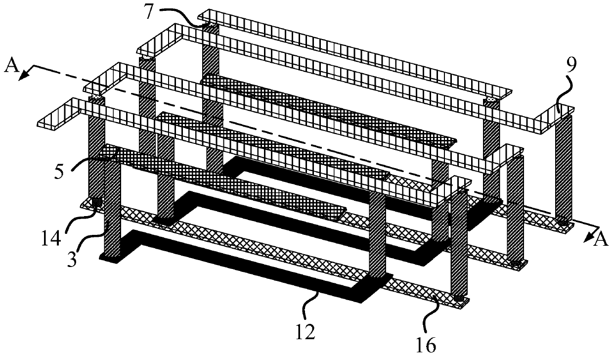
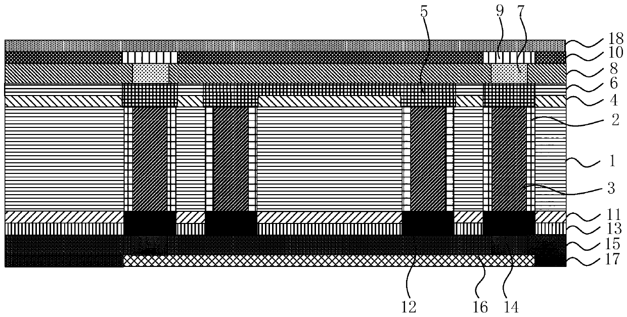
[0046] See also figure 1 and figure 2 , figure 1 A schematic structural diagram of a compact nested inductor structure based on through-silicon vias provided by an embodiment of the present invention; figure 2 for figure 1 Schematic diagram of the cross-sectional structure of AA in . It should be noted, figure 1 In order to better represent the compact nested inductance structure, only a structural schematic diagram of the metal part of the compact nested inductance structure is shown, the semiconductor substrate 1, the annular dielectric layer 2, the first isolation layer 4, the fourth isolation layer 8, The fifth isolation layer 10 , the second isolation layer 11 , the second isolation layer 11 , the sixth isolation layer 13 , the seventh isolation layer 15 , the eighth isolation layer 17 and the passivation layer 18 are not shown.

[0047] A TSV-based compact nested inductor structure comprising:

[0048] semiconductor substrate 1;

[0049] through-silicon vias loc...

Embodiment 2

[0088] On the basis of the above-mentioned embodiments, this embodiment describes in detail a method for manufacturing a compact nested inductor structure based on TSVs.

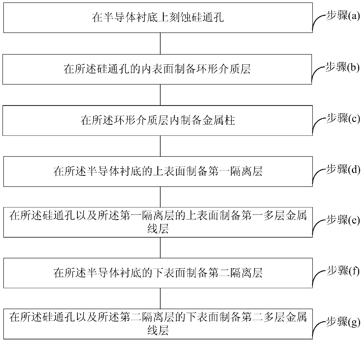
[0089] See image 3 , image 3 A schematic flow chart of a method for preparing a compact nested inductor structure based on through-silicon vias provided by an embodiment of the present invention, the method includes the following steps:

[0090] Step a: Etching TSVs on the semiconductor substrate 1 .

[0091] Further, several through-silicon vias with a radius of 2.1-12 μm are etched on the semiconductor substrate 1 by reactive ion etching.

[0092] Step b: preparing an annular dielectric layer 2 on the inner surface of the TSV.

[0093] Further, an annular dielectric layer 2 with a thickness of 0.1-2 μm is prepared on the inner surface of the TSV. The function of the annular dielectric layer 2 is to realize electrical isolation between the semiconductor substrate 1 and the TSV, thereby reducing the imp...

Embodiment 3

[0126] see again figure 1 and figure 2 , the embodiment of the present invention provides another description of the compact nested inductor structure.

[0127] The compact nested inductor structure includes: a semiconductor substrate 1, through-silicon vias, an annular dielectric layer 2, metal pillars 3, a first isolation layer 4, a first metal line layer 5, a third isolation layer 6, and a first metal via Layer 7, the fourth isolation layer 8, the second metal line layer 9, the fifth isolation layer 10, the second isolation layer 11, the third metal line layer 12, the sixth isolation layer 13, the second metal via layer 14, the second The seventh isolation layer 15 , the fourth metal line layer 16 , the eighth isolation layer 17 , and the passivation layer 18 .

[0128] Wherein, the TSV is located inside the semiconductor substrate 1 , the metal pillar 3 is located inside the TSV, and the annular dielectric layer 3 is located between the metal pillar 4 and the TSV.

[0...


PUM

PropertyMeasurementUnit
radiusaaaaaaaaaa
thicknessaaaaaaaaaa
thicknessaaaaaaaaaa

Abstract

The invention relates to a through-silicon-via-based compact nested inductor structure and a preparation method thereof; the compact nested inductor structure comprises a semiconductor substrate, a through silicon via, an annular dielectric layer, a metal column, a first isolation layer, a first multilayer metal wire layer, a second isolation layer and a second multilayer metal wire layer, whereinthe through silicon via is located in the semiconductor substrate, and the two ends of the through silicon via penetrate through the semiconductor substrate; the annular dielectric layer is positioned on the inner surface of the through silicon via; the metal column is positioned in the annular dielectric layer; the first isolation layer is positioned on the upper surface of the semiconductor substrate; the first multilayer metal wire layer is positioned in the through silicon via and on the upper surface of the first isolation layer; the second isolation layer is located on the lower surfaceof the semiconductor substrate; and the second multilayer metal wire layer is located in the through silicon via and on the lower surface of the second isolation layer. According to the compact nested inductor structure, nesting of two inductor spiral rings is realized on the basis of a traditional through silicon via three-dimensional inductor, so that the effect of increasing the inductance density is achieved.

Description

technical field [0001] The invention belongs to the field of three-dimensional integrated circuits, and in particular relates to a compact nested inductance structure based on through-silicon holes and a preparation method thereof. Background technique [0002] With the development of microelectronics technology, the feature size of semiconductor devices is gradually decreasing, and the integration level of integrated circuits is gradually increasing. Moore's Law is being challenged more and more, mainly including: the feature size of transistors gradually reaches the process limit, quantum effects and short channel effects are becoming more and more serious; as the operating frequency becomes higher and higher, timing problems caused by parasitic effects such as interconnection resistance, capacitance and inductance; power consumption caused by connection capacitance, leakage current and short circuit ; Coupling and crosstalk caused by excessive interconnect density; reliab...

Claims


Application Information

Patent Timeline
Patent Type & Authority Patents(China)
IPC IPC(8): H01L23/64
Inventor 朱樟明曲晨冰刘阳刘晓贤卢启军尹湘坤
Owner XIDIAN UNIV
Why Eureka
Try Eureka