Quantum dot LED package structure and packaging method

A technology of LED encapsulation and encapsulation method, which is applied in the direction of electrical components, circuits, semiconductor devices, etc., can solve the problems of low luminous efficiency and short life of quantum dot LEDs, solve the problems of water and oxygen isolation and heat insulation, and improve stability Sexuality and cost reduction effect

Active Publication Date: 2019-05-14
SOUTH CHINA NORMAL UNIVERSITY
View PDF3 Cites 4 Cited by
  • Summary
  • Abstract
  • Description
  • Claims
  • Application Information

AI Technical Summary

Problems solved by technology

[0003] The purpose of the present invention is to address the deficiencies of the prior art and provide a quantum dot LED packaging structure, which effectively solves the technical problem of the existing quantum dot LED with low luminous efficiency and short lifespan.

Method used


Image

  • Quantum dot LED package structure and packaging method
  • Quantum dot LED package structure and packaging method
  • Quantum dot LED package structure and packaging method

Examples


Embodiment 1

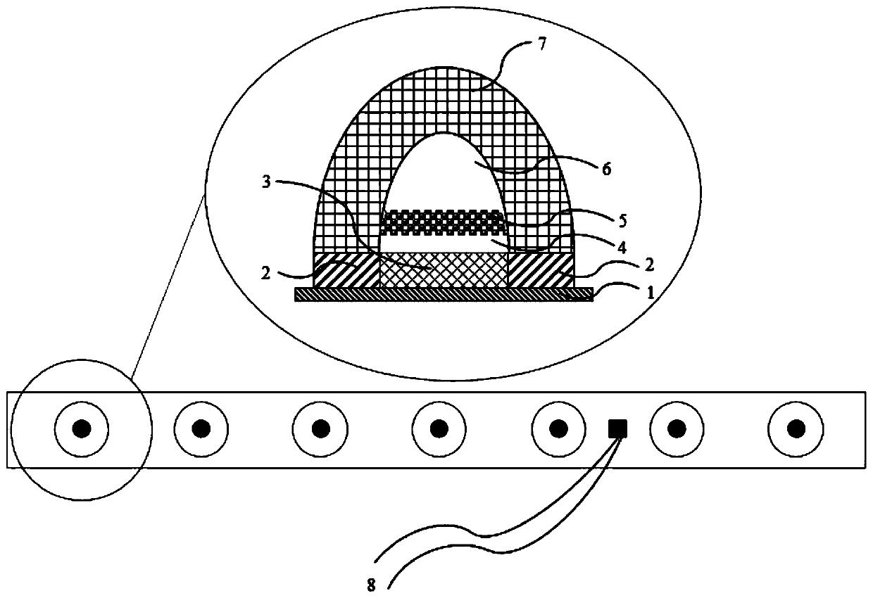
[0051] Such as figure 1 As shown, the present embodiment provides a quantum dot LED package structure, the package structure comprising:

[0052] Blue LED chip (3);

[0053] A strip substrate (1) for fixing the blue LED chip (3);

[0054] connecting the blue LED chip (3) and the electrode (2) of the strip substrate (1);

[0055] Curing the AB glue heat insulation layer (4) on the upper surface of the blue LED chip (3);

[0056] Curing the quantum dot layer (5) on the upper surface of the AB glue heat insulation layer (4);

[0057] Curing the AB glue protective layer (6) on the upper surface of the quantum dot layer (5);

[0058] Cover the blue LED chip (3), electrode (2), AB glue heat insulation layer (4), quantum dot layer (5) and AB glue protective layer (6) and align the above components with the strip substrate (1) A sealed PMMA lens encapsulation layer (7);

[0059]A common electrode (8) arranged on the strip substrate (1) and connecting each blue LED chip (3) in se...

Embodiment 2

[0064] This embodiment provides a packaging method for a quantum dot LED packaging structure, the flow chart of the method is as follows Figure 4 shown, including the following steps:

[0065] S1, fixing the blue LED chip (3) on the strip substrate (1);

[0066] S2. Connect the electrode (2) of each blue LED chip (3) to the strip substrate (1);

[0067] S3, inject AB glue into PMMA lens groove bottom and solidify, form AB glue protective layer (6);

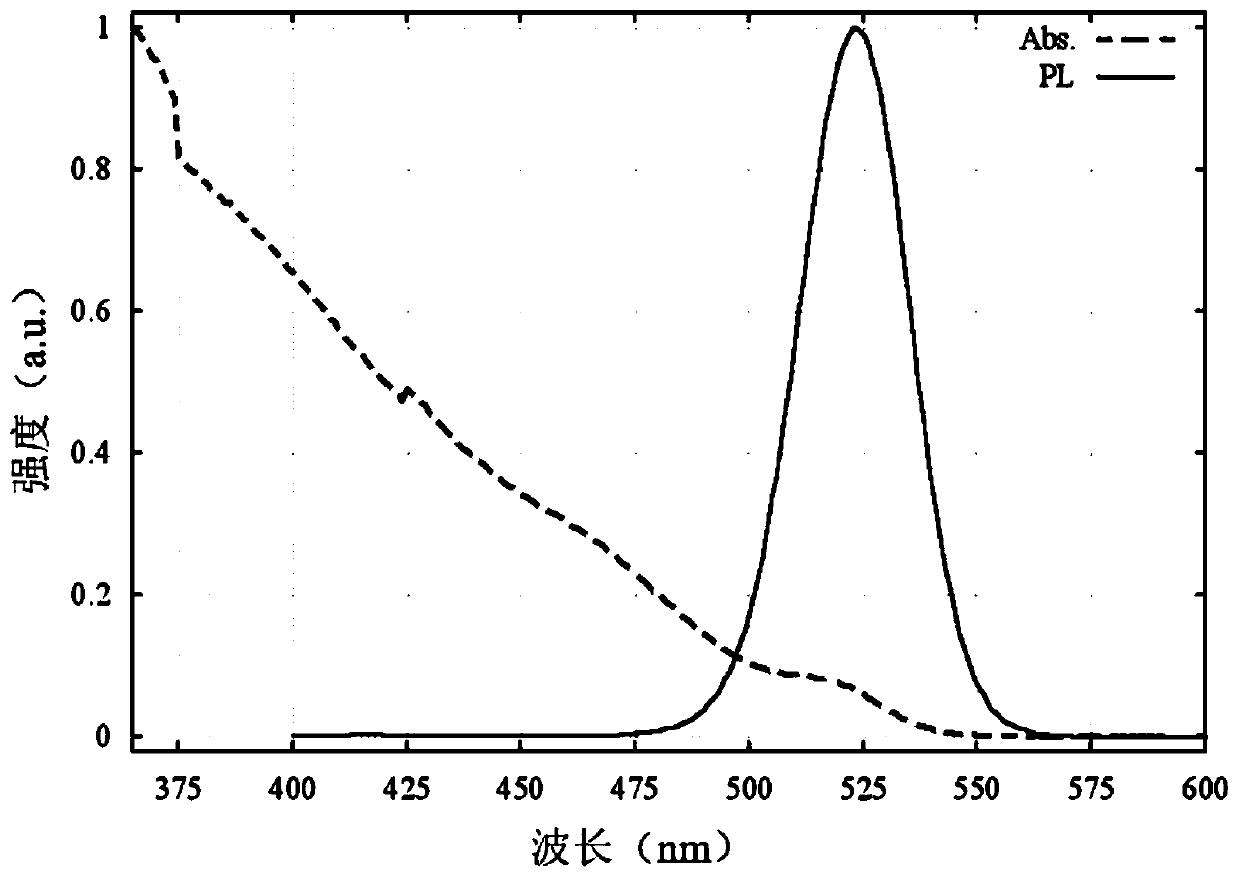
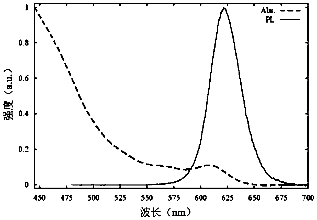
[0068] S4, continue to inject the AB glue that is mixed with CdSe red and green photon quantum dots in PMMA lens groove and solidify, form quantum dot layer (5);

[0069] S5, continue to fill with AB glue in PMMA lens groove and solidify, form AB glue insulation layer (4);

[0070] S6. Apply UV glue to the edge of the filled PMMA lens and fix it directly above the blue LED chip (3) and then cure, and connect each blue LED chip (3) in series through the common electrode (8) to complete the quantum dot LED packaging structure p...


PUM


Abstract

The invention discloses a quantum dot LED package structure and a packaging method. The package structure comprises the following parts of blue LED chips; a strip substrate for fixing the blue LED chips; an electrode connecting the blue LED chips and the strip substrate; an AB adhesive insulation layer cured on the upper surfaces of the blue LED chips; a quantum dot layer cured on the upper surface of the AB adhesive insulation layer; an AB adhesive protective layer cured on the upper surface of the quantum dot layer; a PMMA lens encapsulation layer covering the blue LED chips, the electrode,the AB adhesive insulation layer, the quantum dot layer and the AB adhesive protective layer and sealing the above components with the strip substrate; and a common electrode disposed on the strip substrate and connecting respective blue LED chips in series. By providing a lens encapsulation layer and a double-layer protective rubber layer, the invention can block the invasion of the quantum dot layer and the LED chips by the external water and oxygen, which provides an environment for isolating water and oxygen for quantum dots and is beneficial to improving the luminous efficiency and service life of the quantum dots.

Description

technical field [0001] The invention relates to the technical field of LED packaging, in particular to a quantum dot LED packaging structure and packaging method. Background technique [0002] In recent years, due to the unique optical properties caused by the quantum confinement effect, semiconductor nanomaterials, especially II-VI nanomaterials, have been favored by more and more researchers. Research on nanomaterials is mainly focused on obtaining tunable interband excitation and improving the luminous efficiency of semiconductors. This research achievement is mainly applied to optical devices, such as light-emitting diodes, laser diodes and photodetectors. Recently, the application of nano-semiconductors has been extended to biomedical and environmental fields, such as luminescent cell labeling, drug delivery and chemical sensors. Since 2012, with the rapid development of the optoelectronic industry, the market demand for quantum dot products has been increasing. Howev...

Claims


Application Information

Patent Timeline
Patent Type & Authority Applications(China)
IPC IPC(8): H01L33/00H01L33/06H01L33/48H01L33/58H01L33/64
Inventor 宿世臣王果杨欣章勇魏志鹏王晓华唐吉龙
Owner SOUTH CHINA NORMAL UNIVERSITY
Why Eureka
Try Eureka