Electronic chip soldering device

A technology for welding devices and electronic chips, which is applied in the direction of electric heating devices, tin feeding devices, auxiliary devices, etc., can solve problems such as connection points and weak welding, and achieve the effect of low proficiency, low requirements, uniform and stable welding effect

Inactive Publication Date: 2019-05-17
NANJING INST OF RAILWAY TECH
View PDF6 Cites 0 Cited by
  • Summary
  • Abstract
  • Description
  • Claims
  • Application Information

AI Technical Summary

Problems solved by technology

Regardless of the welding method, there is a greater requirement for proficiency in the operation, and there will always be problems such as joints and weak welding in welding operations

Method used


Image

  • Electronic chip soldering device
  • Electronic chip soldering device
  • Electronic chip soldering device

Examples


Embodiment

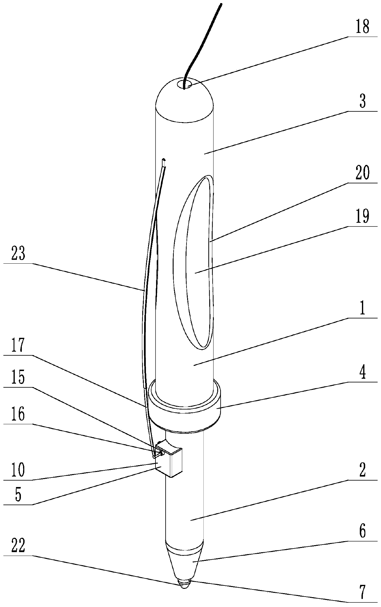
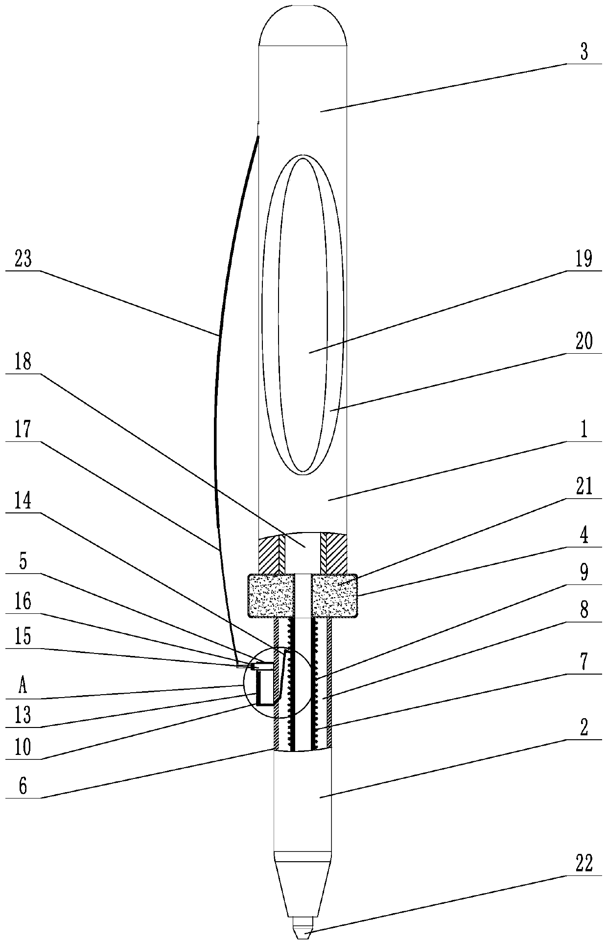
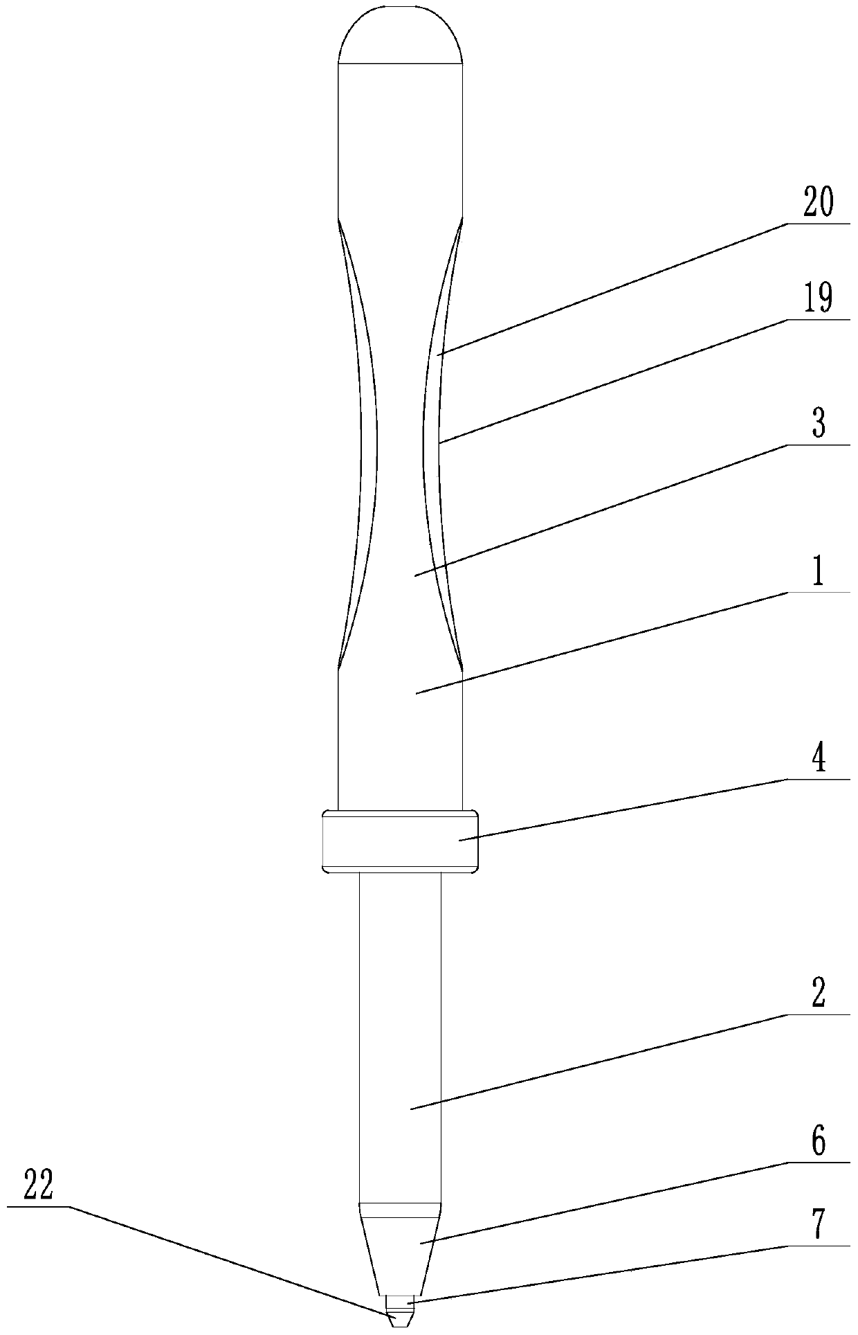
[0038]An electronic chip soldering device includes a soldering pen body 1, the soldering pen body 1 includes a soldering portion 2 and a hand-held portion 3, the soldering portion 2 is located below the hand-held portion 3, and between the soldering portion 2 and the hand-held portion 3 A connecting portion 4 is provided, and a hot-melting portion 5 is provided on the welding portion 2 . The welded portion 2 includes an outer layer 6 and an inner tube 7, and the outer layer and the inner tube are both made of metal. Between the outer layer 6 and the inner tube 7 is a heating chamber 8 , and the tops of the outer layer 6 and the inner tube 7 are welded to the connecting portion 4 . The outer layer 6 is tapered, the diameter of the outer layer 6 gradually decreases from top to bottom, a through hole is formed at the bottom of the outer layer, the through hole passes through the heating chamber 8, and the inner tube 7 passes through the through hole Exposed to the outside, a hea...


PUM


Abstract

The invention provides an electronic chip soldering device, and mainly relates to the field of electronic chip devices. The electronic chip soldering device includes a soldering pen body, the soldering pen body includes a soldering portion and a hand-held portion, a connecting portion is arranged between the soldering portion and the hand-held portion, and a hot-melting portion is arranged on thesoldering portion; the soldering portion includes an outer layer and an inner pipe, and a heating chamber is arranged between the outer layer and the inner pipe; and the hot-melting portion includes ahot-melting shell, a hot-melting chamber and a heating chamber are arranged in the hot-melting shell, the heating chamber is internally provided with an electric heating sheet, a slide way is arranged on the top of the hot-melting chamber, a piston is arranged in the slide way, and an elastic pressing piece is arranged at the end, located on the outer side, of the piston. The electronic chip soldering device has the beneficial effects that operation is simpler, the requirement for proficiency is lower, and the welding effect is more uniform and stable.

Description

technical field [0001] The invention mainly relates to the field of electronic chip equipment, in particular to an electronic chip welding device. Background technique [0002] In the operation class of electronic electrician, it is necessary to train the welding of electronic chips. In manual soldering, generally tin the pads on one side of the pcb board, then clamp the components with tweezers, place them on the tinned pads, and use a soldering pen to heat the tinned pads, components One end has been fixed, and then the two sides are tinned with solder wire. Or when soldering some small components, first use tin wire to tin the soldering iron head, then use tweezers to place the components on the pad, and then use the tin on the soldering iron head to fix the components, and finally fill the two ends with tin. . No matter which welding method is used, there is a large proficiency requirement for the operation, and there will always be problems such as connection points ...

Claims


Application Information

Patent Timeline
Patent Type & Authority Applications(China)
IPC IPC(8): B23K3/053B23K3/06B23K3/08
Inventor 朱颖莉
Owner NANJING INST OF RAILWAY TECH
Why Eureka
Try Eureka