
A bridging method for ahb bus to access on-chip sram

A bus and bridging technology, applied in the bridging field of AHB bus access to on-chip SRAM, can solve the problem of low timing efficiency, and achieve the effects of optimizing timing, improving data transmission efficiency and improving efficiency

Active Publication Date: 2020-07-28
ZHEJIANG UNIV
View PDF6 Cites 0 Cited by
  • Summary
  • Abstract
  • Description
  • Claims
  • Application Information

AI Technical Summary

Problems solved by technology

The usual processing method is to avoid conflicts caused by read-after-write situations by blocking, but this relatively direct method also leads to low timing efficiency

Method used


Image

  • A bridging method for ahb bus to access on-chip sram
  • A bridging method for ahb bus to access on-chip sram
  • A bridging method for ahb bus to access on-chip sram

Examples


Embodiment Construction

[0021] The technical solution of the present invention will be further described below in conjunction with the accompanying drawings.

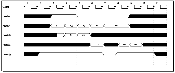
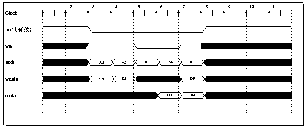
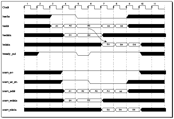
[0022] The method proposed in this patent is a bridge method for AHB bus to access on-chip SRAM. The characteristics of this method are: during the read operation, since the timing of the AHB is the same as that of the SRAM, so in the case of only a read operation in a section of transmission, the control signal of the AHB terminal can be directly connected with the control signal of the SRAM terminal, and the data signal of the AHB terminal can be connected with the control signal of the SRAM terminal. The data signal at the SRAM end is directly connected; during the write operation, since the timing of AHB is to initiate the control signal in the previous beat, and then transmit the data in the next beat, and the timing of the SRAM is that the control signal and the write data are accepted in the same cycle, so in a period of transmission In...


PUM


Abstract

The invention discloses a bridging method for accessing an on-chip SRAM (static random access memory) by an AHB (advanced high performance bus), and belongs to the field of read-write time sequence optimization of data in SOC (system on chip) design. Reading operation: under the condition that only the reading operation exists in one section of transmission, the control signal of the AHB end is directly connected with the control signal of the SRAM end for transmission, and the data signal of the AHB end is directly connected with the data signal of the SRAM end for transmission; Write operation: under the condition that only write operation exists in a section of transmission, registering a control signal and an address signal of the AHB end for a period, and transmitting the control signal and the address signal to the SRAM together with the data in the next beat; And reading after writing: under the condition that both reading operation and writing operation are transmitted in one section and reading after writing occurs, registering a control signal and data of the writing operation, temporarily not transmitting the control signal and the data to the SRAM, and directly transmitting the control signal initiated by the reading operation in the next period to the SRAM. According to the method, the time sequence under the condition of reading after writing can be optimized, andcompared with a common processing method, the method provided by the invention does not need to block the reading operation and optimizes the time sequence of one period.

Description

technical field [0001] The invention relates to the field of timing optimization of data reading and writing in SOC design, in particular to a bridge method for AHB bus to access on-chip SRAM in the data reading and writing process of a processor or DMA. Background technique [0002] SoC is a system chip, also known as a system on a chip (SoC, System on Chip). With the development of integrated circuit design and manufacturing technology, the main functions of the entire system can be integrated on one chip, which is the origin of the system on chip. Compared with the traditional design method, the main advantages of SoC are: more complex system can be realized, lower design cost, higher reliability, shorter product design time and low power consumption can be achieved. With the continuous improvement of integrated circuit manufacturing technology, more quantities and types of devices can be integrated on SoC. At the same time, people's demand for high performance of SoC wi...

Claims


Application Information

Patent Timeline
Patent Type & Authority Patents(China)
IPC IPC(8): G06F30/20
Inventor 黄凯陈子旋余慜修思文
Owner ZHEJIANG UNIV
Features
  • Generate Ideas
  • Intellectual Property
  • Life Sciences
  • Materials
  • Tech Scout
  • Unparalleled Data Quality
  • Higher Quality Content
  • 60% Fewer Hallucinations
Learn More