

FPGA design circuit diagram generation method and device, computer equipment and storage medium
A technology for circuit design and user design, applied in the field of FPGA development, can solve problems such as complex wiring structures, achieve clear structure, reduce complexity, and reduce memory usage
- Summary
- Abstract
- Description
- Claims
- Application Information
AI Technical Summary
Problems solved by technology
Method used
Image

Examples
Embodiment Construction
[0035] The following will clearly and completely describe the technical solutions in the embodiments of the present invention with reference to the accompanying drawings in the embodiments of the present invention. Obviously, the described embodiments are part of the embodiments of the present invention, but not all of them. Based on the embodiments of the present invention, all other embodiments obtained by persons of ordinary skill in the art without creative efforts fall within the protection scope of the present invention.
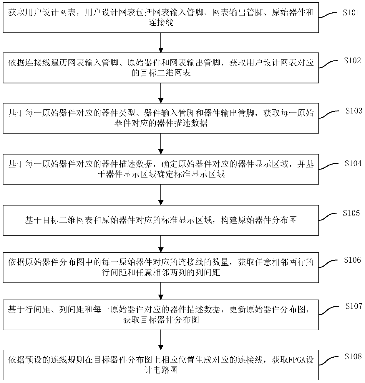
[0036] The FPGA design circuit diagram generation method provided by the embodiment of the present invention, the FPGA design circuit diagram generation method is applied in the FPGA editing and development system, and is used to develop and design an FPGA design circuit diagram with a simple wiring structure, so as to reduce the software memory occupation and improve the FPGA design circuit diagram. development efficiency.
[0037] In one embodiment, ...
PUM
 Abstract
Description
Claims
Application Information