Device and method for debugging orthogonality of positioning motion platform of direct writing lithography exposure equipment

A technology for positioning motion and motion platform is applied in the field of orthogonality debugging device for positioning motion platform of direct writing lithography exposure equipment, which can solve the problems of increased cost, high price, and extremely high test environment requirements, so as to reduce splicing dislocation and improve efficiency. and accuracy, reducing the effect of debugging costs

Pending Publication Date: 2019-06-07
HEFEI CHIP FOUND MICROELECTRONICS EQUIP CO LTD
View PDF0 Cites 9 Cited by
  • Summary
  • Abstract
  • Description
  • Claims
  • Application Information

AI Technical Summary

Problems solved by technology

[0004] The traditional direct-writing lithography exposure equipment precision positioning motion platform orthogonality debugging method mainly uses the verticality measurement module of the laser interferometer to measure the orthogonality values ​​​​of different positions of the XY-axis integrated platform plane along the axis running direction. A mirror whose length can cover the travel of the XY axis is required, and the cost is further increased. This method is expensive, the test environment is extremely demanding, and the assembly and debugging process is complicated

Method used


Image

  • Device and method for debugging orthogonality of positioning motion platform of direct writing lithography exposure equipment
  • Device and method for debugging orthogonality of positioning motion platform of direct writing lithography exposure equipment
  • Device and method for debugging orthogonality of positioning motion platform of direct writing lithography exposure equipment

Examples


Embodiment Construction

[0040] The present invention will be further described below in conjunction with accompanying drawing:

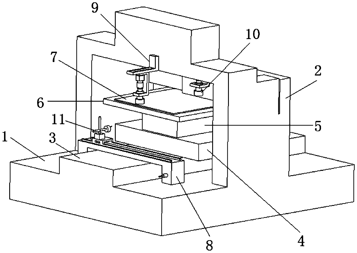
[0041] Such as figure 1 The shown direct writing lithography exposure equipment positioning motion platform orthogonality debugging device includes a support base 1, a precision positioning motion platform installed on the support base 1, a debugging mechanism installed on the support base 1, and a support base 1 The supporting frame 2 and the CCD image acquisition system installed on the supporting frame 2.

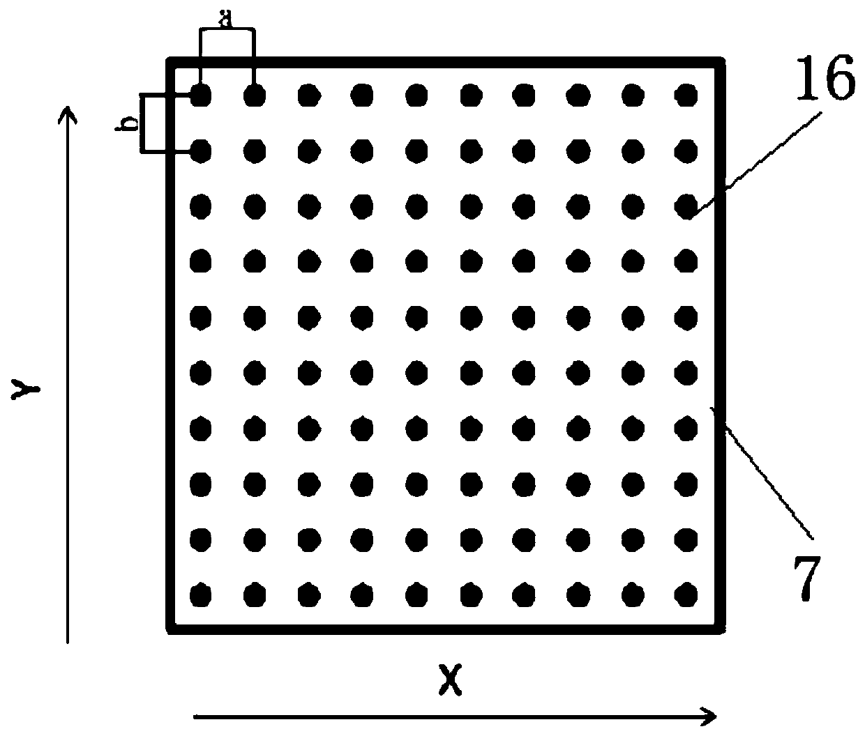
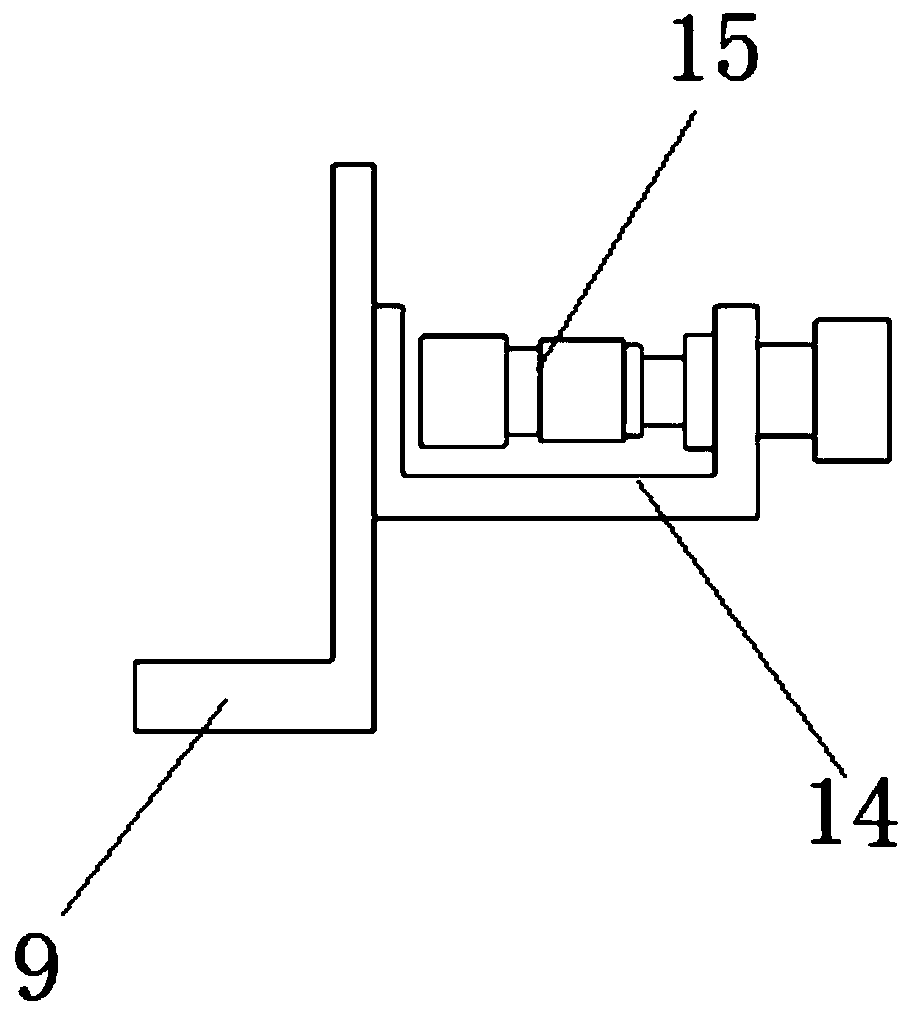
[0042] The precision positioning motion platform includes a Y-axis 3, an X-axis 4 and a Z-axis 5 arranged sequentially from bottom to top. The structure of the precision positioning motion platform is the same as the structure of the precision positioning motion platform used in the direct writing lithography exposure equipment in the prior art. A vacuum chuck 6 is installed on the top of the Z-axis 5 ; a high-precision calibration plate 7 is placed above the vacuum c...


PUM


Abstract

The invention relates to a device and method for debugging orthogonality of a positioning motion platform of direct writing lithography exposure equipment, and belongs to the technical field of directwriting lithography exposure. The debugging device comprises a support base, a precision positioning motion platform, a debugging mechanism, a support frame and a CCD image acquisition system, wherein the precision positioning motion platform comprises a Y-axis, an X-axis and a Z-axis; a vacuum suction cup is mounted on the top of the Z-axis; and a high-precision calibration plate with a Mark point is adsorbed above the vacuum suction cup. The debugging mechanism comprises a movable sliding table capable of lifting mounted on the support base, a debugging connection bottom plate, a movable sliding rail, a movable sliding rail motion seat slidingly matched with the movable sliding rail, and a dial gauge fixed on the movable sliding rail motion seat. The device and method, by first adoptinga CCD image acquisition system to measure the orthogonality of the X-axis and the Y-axis, and then using a debugging mechanism to debug the orthogonality of the X-axis and the Y-axis, can improve theefficiency and accuracy of the orthogonality debugging of the precision positioning motion platform of the direct writing lithography exposure equipment, and reduce the debugging cost.

Description

technical field [0001] The invention relates to the technical field of direct writing lithography exposure, in particular to a device and method for adjusting the orthogonality of a positioning motion platform of a direct writing lithography exposure device. Background technique [0002] Direct write lithography is the use of lasers to print characteristic patterns on the surface of a substrate. Such substrates are used in fields such as PCB circuit boards, semiconductor devices, flat panel displays, biochips, packages, and microelectronic chips. The process of direct writing lithography plate making on the substrate is: place the substrate on the vacuum chuck of the precision positioning motion platform, use vacuum adsorption, and project the designed characteristic pattern onto the substrate surface through the exposure device in the lithography equipment, In order to ensure that the pattern exposed on the substrate is consistent with the theoretical pattern, the trajecto...

Claims


Application Information

Patent Timeline
Patent Type & Authority Applications(China)
IPC IPC(8): G03F7/20
Inventor 李辉项宗齐卫攻文
Owner HEFEI CHIP FOUND MICROELECTRONICS EQUIP CO LTD
Why Eureka
Try Eureka