Image sensor and formation method

An image sensor and graphic technology, applied in the direction of radiation control devices, etc., can solve the problems of poor image sensor performance and low photosensitivity, and achieve the effects of improving photoelectric conversion efficiency, sensitivity, and photosensitivity

Inactive Publication Date: 2019-06-11
HUAIAN IMAGING DEVICE MFGR CORP
View PDF3 Cites 2 Cited by
  • Summary
  • Abstract
  • Description
  • Claims
  • Application Information

AI Technical Summary

Problems solved by technology

[0004] However, the photosensitivity of the image sensor is not high in low-lig

Method used


Image

  • Image sensor and formation method
  • Image sensor and formation method
  • Image sensor and formation method

Examples


Embodiment Construction

[0025] As mentioned in the background, prior art image sensors perform poorly.

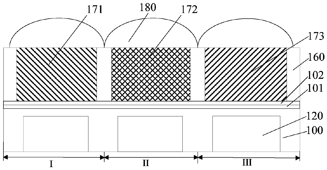
[0026] figure 1 It is a schematic diagram of the cross-sectional structure of an image sensor.

[0027] An image sensor, reference figure 1 , comprising: a semiconductor substrate 100 having opposite first and second surfaces; a photosensitive structure 120 located in the semiconductor substrate 100, the first surface of the semiconductor substrate 100 exposing the photosensitive structure 120 The anti-reflection coating 101 positioned on the second surface of the semiconductor substrate 100; the anti-reflection layer 102 positioned on the surface of the anti-reflection coating 101; Filter layer and lens layer 180.

[0028] figure 1 shows three pixel units of the image sensor, including green pixel unit I, blue pixel unit II and red pixel unit III.

[0029] The filter layer located in the green pixel unit I is the G filter layer 171; the filter layer located in the blue pixel unit II is the B...


PUM

PropertyMeasurementUnit
Thicknessaaaaaaaaaa

Abstract

The invention relates to an image sensor and a formation method. The method comprises the steps of providing a semiconductor substrate, wherein the semiconductor substrate comprises a first surface and a second surface which are opposite to each other, and the semiconductor substrate comprises a plurality of first regions; forming a conversion light-emitting material layer on a surface of the second surface at each first region of the semiconductor substrate; and forming a filtering structure on surfaces of the conversion light-emitting material layer and the second surface of the semiconductor substrate. By the method, the performance of the image sensor is improved.

Description

technical field [0001] The invention relates to the field of image sensor manufacturing, in particular to an image sensor and a forming method thereof. Background technique [0002] An image sensor is a semiconductor device that converts light signals into electrical signals. Image sensors are classified into complementary metal oxide (CMOS) image sensors and charge coupled device (CCD) image sensors. CMOS image sensor has the advantages of simple process, easy integration with other devices, small size, light weight, low power consumption and low cost. At present, CMOS image sensors have been widely used in still digital cameras, digital video cameras, medical imaging devices, and automotive imaging devices. [0003] CMOS image sensors include front illuminated (FSI) image sensors and back illuminated (BSI) image sensors. In a back-illuminated image sensor, light is incident on photodiodes in the image sensor from the back of the image sensor, thereby converting light en...

Claims


Application Information

Patent Timeline
IPC IPC(8): H01L27/146
Inventor 姜怡雯孟俊生李志伟
Owner HUAIAN IMAGING DEVICE MFGR CORP
Why Eureka
Try Eureka