Three-dimensional memory and manufacture method thereof

A manufacturing method and memory technology, applied in the direction of electric solid-state devices, semiconductor devices, electrical components, etc., can solve the problems of poor retention characteristics of three-dimensional memory, and achieve the effect of improving retention characteristics

Active Publication Date: 2019-06-14
YANGTZE MEMORY TECH CO LTD
View PDF13 Cites 11 Cited by
  • Summary
  • Abstract
  • Description
  • Claims
  • Application Information

AI Technical Summary

Problems solved by technology

[0005] The invention provides a three-dimensional memory and its manufacturing method, which are used to solve the problem of poor retention characteristics of the existing three-dimensional memory

Method used


Image

  • Three-dimensional memory and manufacture method thereof
  • Three-dimensional memory and manufacture method thereof
  • Three-dimensional memory and manufacture method thereof

Examples


Embodiment Construction

[0046] The specific implementation of the three-dimensional memory and its manufacturing method provided by the present invention will be described in detail below in conjunction with the accompanying drawings.

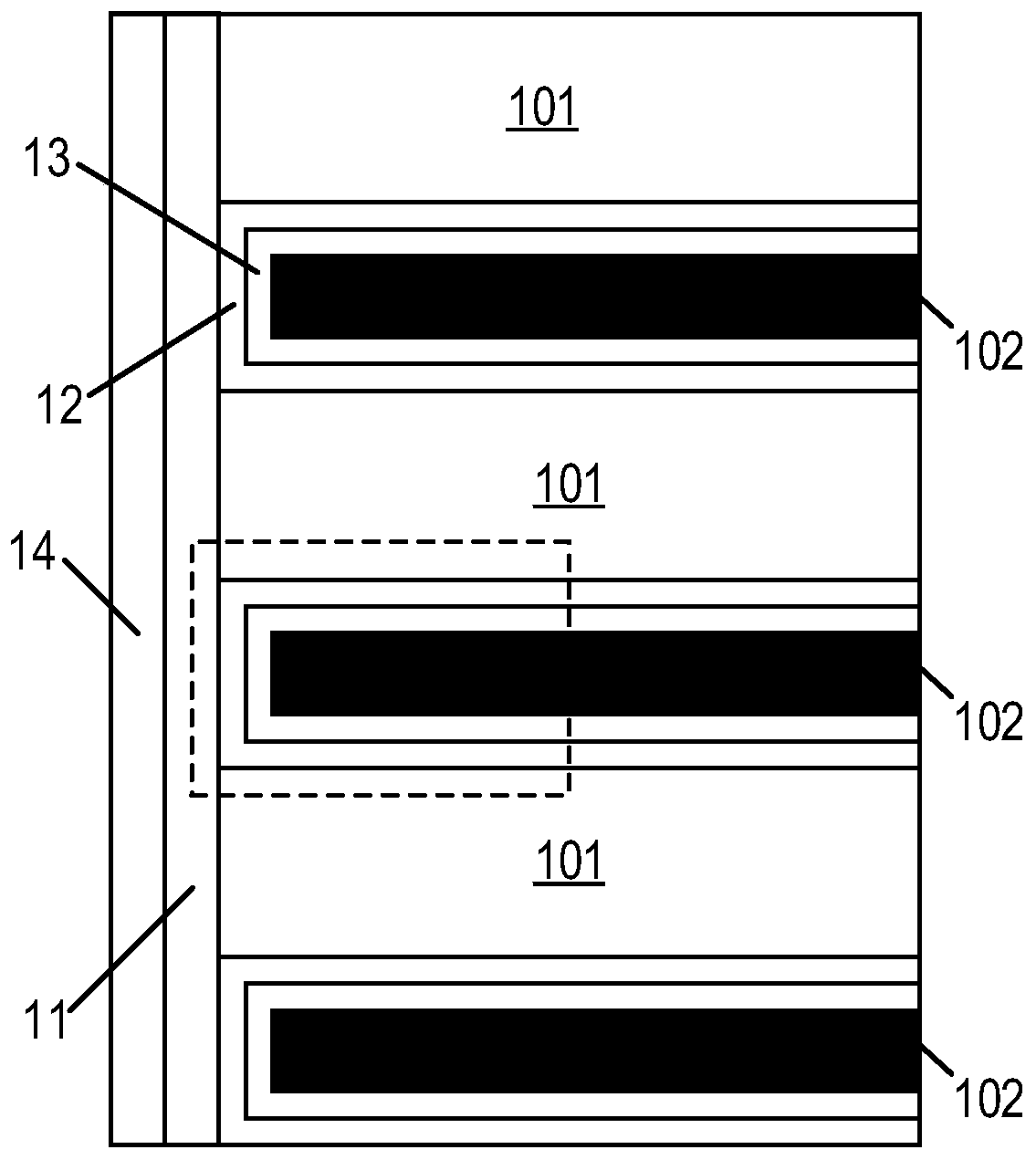
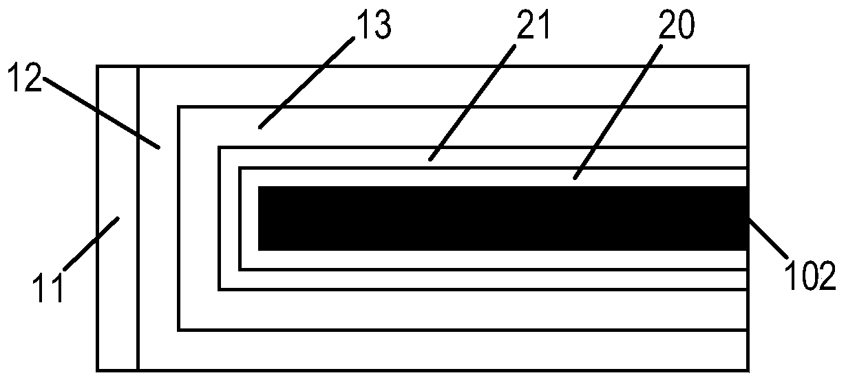
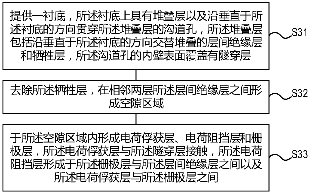
[0047] In the existing three-dimensional memory such as 3D NAND, the storage string as its key storage structure is composed of a blocking layer, a charge trapping layer, a tunneling layer and channel layer. After sequentially depositing the blocking layer, the charge trapping layer and the tunneling layer in the channel hole, the blocking layer, the charge trapping layer and the tunneling layer are etched to open The epitaxial semiconductor layer is exposed at the bottom of the channel hole; then the channel layer is deposited to form a channel path, thereby controlling the charge storage function of the three-dimensional memory.

[0048] As the market's requirements for storage density continue to increase, the number of stacked layers in the stacked structure in t...


PUM


Abstract

The invention relates to the technical field of semiconductor manufacture, in particular to a three-dimensional memory and a manufacture method thereof. The three-dimensional memory comprises a substrate, a tunneling layer, a plurality of charge capture layers and a plurality of charge barrier layers, wherein the substrate is provided with a stacking structure and channel holes which penetrate through the stacking structure along a direction vertical to the substrate, the stacking structure comprises interlayer insulation layers and grid electrode layers, and the interlayer insulation layers and the grid electrode layers are alternately stacked along a direction vertical to the substrate; the tunneling layer covers the inner wall surface of the channel holes; each charge capture layer is positioned between two adjacent interlayer insulation layers and is in contact with the tunneling layer; and each charge barrier layer is positioned between each grid electrode layer and each interlayer insulation layer as well as each charge capture layer and each grid electrode layer. By use of the three-dimensional memory, the migration of current carriers in the charge capture layers along a channel direction can be prevented, and the retention characteristics of the three-dimensional memory are improved.

Description

technical field [0001] The invention relates to the technical field of semiconductor manufacturing, in particular to a three-dimensional memory and a manufacturing method thereof. Background technique [0002] As technology develops, the semiconductor industry is constantly seeking new ways to produce a greater number of memory cells per memory die in a memory device. In non-volatile memory, such as NAND memory, one way to increase the memory density is by using vertical memory arrays, that is, 3D NAND (three-dimensional NAND) memory; 32 layers developed to 64 layers, or even higher layers. [0003] In a 3D NAND memory, there is a stack structure formed by alternately stacking interlayer insulating layers and gates, and the stack structure includes a core area and a stepped area surrounding the core area. The core area is used for storing information; the step area is located at the end of the stack structure and is used for transmitting control information to the core are...

Claims


Application Information

Patent Timeline
Patent Type & Authority Applications(China)
IPC IPC(8): H01L27/1157H01L27/11582
Inventor 王启光
Owner YANGTZE MEMORY TECH CO LTD
Why Eureka
Try Eureka