3D NAND memory device and manufacturing method thereof

A storage device and manufacturing method technology, which is applied to electric solid-state devices, semiconductor devices, electrical components, etc., can solve the problems of enhancing mutual influence and reducing the characteristics of storage devices, so as to improve retention characteristics, reduce mutual influence, and prevent migration. Effect

Inactive Publication Date: 2020-07-28
YANGTZE MEMORY TECH CO LTD
View PDF3 Cites 2 Cited by
  • Summary
  • Abstract
  • Description
  • Claims
  • Application Information

AI Technical Summary

Problems solved by technology

With the continuous improvement of storage density requirements, the number of stacked layers in the stacked structure continues to increase. In order to reduce the impact of stress and control costs, the thickness of each single layer in the stacked layer is continuously reduced, resulting in the mutual influence between the memory cells. Enhanced, in turn degraded memory device characteristics

Method used


Image

  • 3D NAND memory device and manufacturing method thereof
  • 3D NAND memory device and manufacturing method thereof
  • 3D NAND memory device and manufacturing method thereof

Examples


Embodiment Construction

[0036] In order to make the above objects, features and advantages of the present invention more comprehensible, specific implementations of the present invention will be described in detail below in conjunction with the accompanying drawings.

[0037] In the following description, a lot of specific details are set forth in order to fully understand the present invention, but the present invention can also be implemented in other ways different from those described here, and those skilled in the art can do it without departing from the meaning of the present invention. By analogy, the present invention is therefore not limited to the specific examples disclosed below.

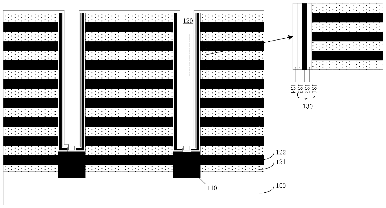
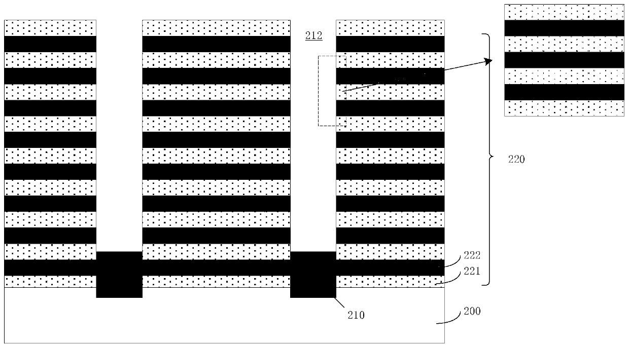
[0038] As described in the background technology, as the requirements for storage density continue to increase, the number of stacked layers in the stacked structure continues to increase. In order to reduce the impact of stress and control costs, the thickness of each single layer in the stacked layer is contin...


PUM


Abstract

The invention provides a 3D NAND memory device. A through channel hole is formed in a stacking layer on a substrate, a gate layer on a side wall of the channel hole is provided with a gap, the gap andan adjacent insulating layer form grooves, a storage function layer is formed in the groove and is positioned between an end surface of the gate layer and the channel layer, thus, storage units are connected through the channel layer, charge storage layers of the storage units are isolated by the insulating layers, so carriers are prevented from migrating along the channel direction, mutual influence among the storage units is reduced, and the retention characteristic of the storage device is improved.

Description

technical field [0001] The invention relates to the field of semiconductor devices and manufacturing, in particular to a 3D NAND storage device and a manufacturing method thereof. Background technique [0002] 3D NAND memory is a flash memory device with a three-dimensional stack structure, and its storage core area is composed of alternately stacked metal gate layers and insulating layers combined with vertical channel transistors. With the continuous improvement of storage density requirements, the number of stacked layers in the stacked structure continues to increase. In order to reduce the impact of stress and control costs, the thickness of each single layer in the stacked layer is continuously reduced, resulting in the mutual influence between the memory cells. Enhance, and then degrade the characteristics of the memory device. Contents of the invention [0003] In view of this, the object of the present invention is to provide a 3D NAND storage device and a manufa...

Claims


Application Information

Patent Timeline
Patent Type & Authority Applications(China)
IPC IPC(8): H01L27/1157H01L27/11582
CPCH10B43/35H10B43/27
Inventor 王启光
Owner YANGTZE MEMORY TECH CO LTD
Why Eureka
Try Eureka