Image sensor and forming method thereof

An image sensor and pixel technology, which is applied in radiation control devices and other directions, can solve the problems that affect the focusing effect of PDAF technology and the optical image sensor cannot work normally, achieve the effect of uniform light transmission and signal amount, and improve the focusing effect

Inactive Publication Date: 2019-06-14
HUAIAN IMAGING DEVICE MFGR CORP
View PDF10 Cites 3 Cited by
  • Summary
  • Abstract
  • Description
  • Claims
  • Application Information

AI Technical Summary

Problems solved by technology

[0005] In the prior art, in order to improve the performance of the optical image sensor, the Phase Detection Auto Focus (PDAF) technology is used for focusing. The PDAF technology focuses based on the principle of phase difference, which helps to increase the focusing speed and improve the focusing effect , to determine the correct position of the lens so that the image is not out of focus, causing the optical image sensor to not work properly
[0006] However, in the prior art, due to differences in the focus spot (Light Spot) at different positions of the image sensor, it will affect the focusing effect of the PDAF technology

Method used


Image

  • Image sensor and forming method thereof
  • Image sensor and forming method thereof
  • Image sensor and forming method thereof

Examples


Embodiment Construction

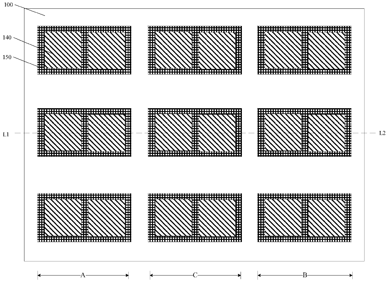
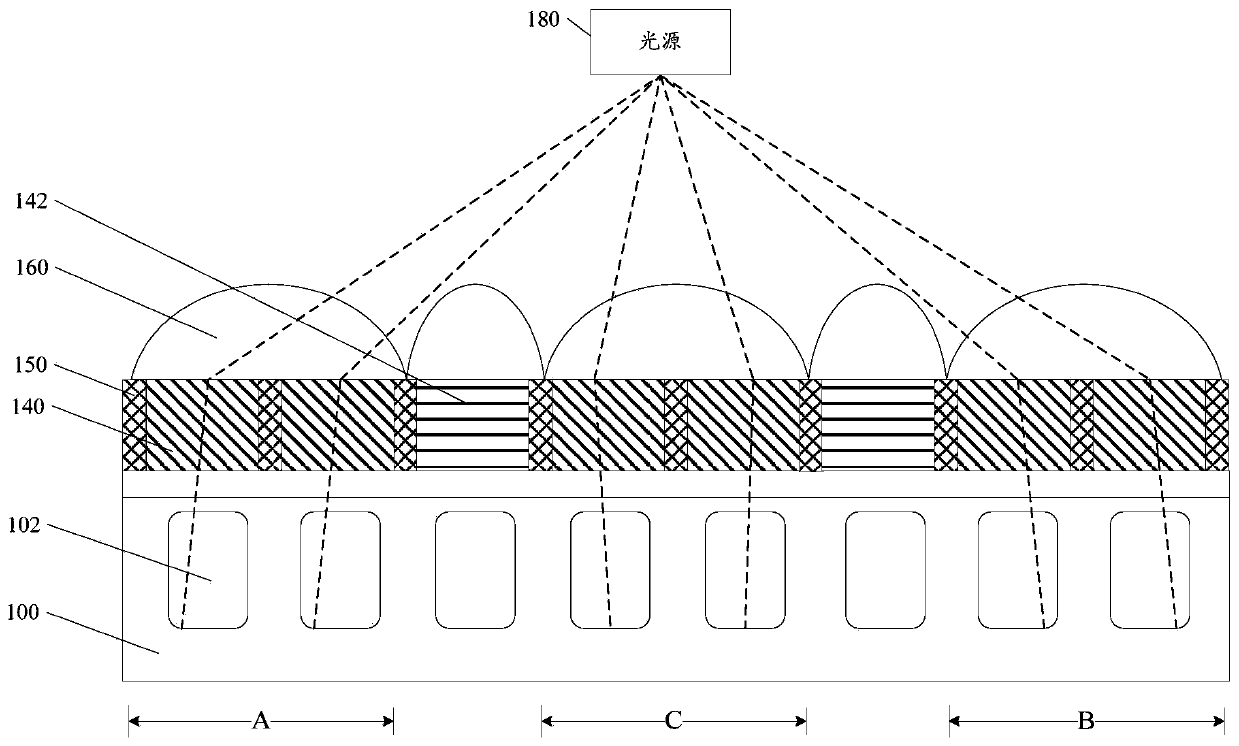
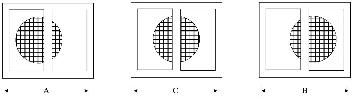
[0030] In the prior art, in order to improve the performance of the optical image sensor, the PDAF technology is used to focus based on the principle of phase difference, which helps to increase the focusing speed, improve the focusing effect, and determine the correct position of the lens to prevent the image from being out of focus. Cause the optical image sensor to not work properly.

[0031] Specifically, in PDAF technology, the light from the light source enters the pixel device (such as a photodiode) in the semiconductor substrate after passing through two pairs of color filters, and then forms a focusing the spots and comparing the focused spots to determine the degree of focus. Specifically, since the focused light spots formed after passing through the two color filters are consistent in intensity, when the focused light spots formed after passing through the two color filters are consistent in area, it can be considered that the focusing requirements are met; when th...


PUM


Abstract

The invention provides an image sensor and a forming method thereof. The image sensor comprises: a semiconductor substrate; a pixel device located in the semiconductor substrate; color filter pairs arranged in rows for PDAF, wherein the color filter pairs are located on the surface of the semiconductor substrate, and each row has a plurality of color filter pairs; in two color filters of each color filter pair, the thickness of the color filter deviating toward the row center of the located row is less than the thickness of the color filter deviating from the row center of the located row; andthe thickness direction is perpendicular to the surface of the semiconductor substrate. The scheme provided by the invention is conducive to compensating the influence caused by the positions of thecolor filters and improving the focusing effect of the PDAF technology.

Description

technical field [0001] The invention relates to the technical field of semiconductor manufacturing, in particular to an image sensor and a forming method thereof. Background technique [0002] The image sensor is the core component of the camera equipment, which realizes the image capture function by converting the optical signal into an electrical signal. Taking a CMOS image sensor (CMOS Image Sensors, CIS) device as an example, due to its advantages of low power consumption and high signal-to-noise ratio, it has been widely used in various fields. [0003] Taking Back-side Illumination (BSI) CIS as an example, in the existing manufacturing process, logic devices and pixel devices are first formed in the semiconductor substrate and metal interconnection structures are formed on the surface of the semiconductor substrate, and then Bonding the carrier wafer with the front side of the semiconductor substrate, and then thinning the back of the semiconductor substrate, and then...

Claims


Application Information

Patent Timeline
Patent Type & Authority Applications(China)
IPC IPC(8): H01L27/146
Inventor 王亮内藤逹也
Owner HUAIAN IMAGING DEVICE MFGR CORP
Why Eureka
Try Eureka