Computational Lithography Method and System for Optical Proximity Correction

A technology of optical proximity effect and computational lithography, which is applied in the field of lithography technology and can solve problems such as increasing time costs

Active Publication Date: 2022-08-02
CHANGXIN MEMORY TECH INC
View PDF1 Cites 0 Cited by
  • Summary
  • Abstract
  • Description
  • Claims
  • Application Information

AI Technical Summary

Problems solved by technology

This means that existing computational lithography methods require time to iteratively recheck the optical proximity correction and hot spot correction steps, increasing the time cost

Method used


Image

  • Computational Lithography Method and System for Optical Proximity Correction
  • Computational Lithography Method and System for Optical Proximity Correction
  • Computational Lithography Method and System for Optical Proximity Correction

Examples


Embodiment Construction

[0050] In the following, only certain exemplary embodiments are briefly described. As those skilled in the art would realize, the described embodiments may be modified in various different ways, all without departing from the spirit or scope of the present invention. Accordingly, the drawings and description are to be regarded as illustrative in nature and not restrictive. Furthermore, the present disclosure may repeat reference numerals and / or reference letters in different instances for the purpose of simplicity and clarity and not in itself indicative of a relationship between the various embodiments and / or arrangements discussed.

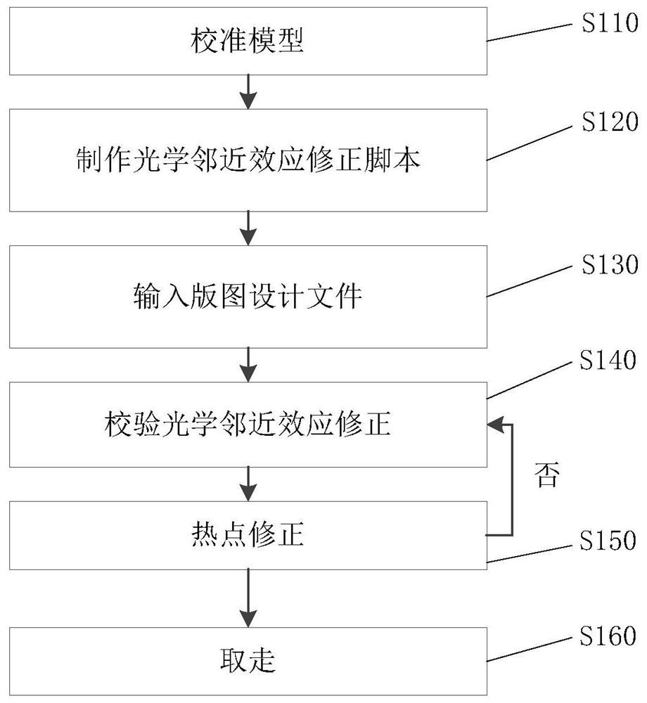
[0051] In the state-of-the-art computational lithography methods, such as figure 1 As shown, the requirement is met after a number of iterations exist between the verification of the optical proximity effect correction and the correction of the hot spot.
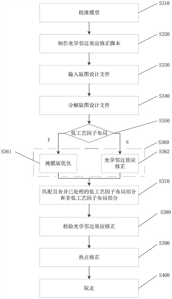
[0052]The basic idea of ​​the embodiments of the present invention is to divide the inpu...


PUM


Abstract

The present invention provides a computational lithography method for optical proximity effect correction. The computational lithography method decomposes the input layout design file into a first layout part and a second layout part according to the value of the process factor, wherein the process factor of the first layout part is lower than a preset threshold, and the second layout part is The process factor of the layout part is greater than the preset threshold; then the first layout part and the second layout part are processed respectively; then, the processed first layout part and the second layout part are matched and merged layout section. Since the first layout part and the second layout part are processed separately, the processing quality is improved, so it is no longer necessary to iteratively perform the step of correcting the optical proximity effect and the step of correcting the hot spot, thereby improving the output speed of the layout design file. The present invention also provides a computational lithography system for optical proximity effect correction.

Description

technical field [0001] The invention relates to a lithography technology in semiconductor manufacturing, in particular to a computational lithography method and system for optical proximity effect correction. Background technique [0002] With the development of semiconductor manufacturing, the integration level is getting higher and higher, and the number of transistors contained in a unit area is also increasing rapidly. The main indicator for measuring integration in the manufacturing process is the resolution of the lithography process, which is used to distinguish the feature patterns adjacent to the surface of the silicon wafer. [0003] As we all know, k1=NA*p / 2λ, where k1 is the process factor or resolution constant; NA (NumericalAperture), the numerical aperture of the optical system of the lithography machine, represents the ability of the lens to collect diffracted light (light-gathering), NA= n*sinθ=n*(lens radius / lens focal length), generally speaking, the size...

Claims


Application Information

Patent Timeline
Patent Type & Authority Patents(China)
IPC IPC(8): G03F1/36
Inventor 不公告发明人
Owner CHANGXIN MEMORY TECH INC
Why Eureka
Try Eureka